SCES626E MARCH 2005 – June 2017 SN74AUC1G19
UNLESS OTHERWISE NOTED, this document contains PRODUCTION DATA.
- 1 Features
- 2 Applications
- 3 Description
- 4 Revision History
- 5 Pin Configuration and Functions
- 6 Specifications
- 7 Parameter Measurement Information
- 8 Detailed Description
- 9 Device and Documentation Support
- 10Mechanical, Packaging, and Orderable Information
封装选项
机械数据 (封装 | 引脚)
散热焊盘机械数据 (封装 | 引脚)
订购信息
5 Pin Configuration and Functions
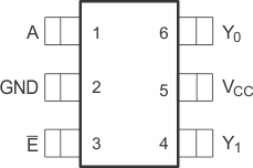
DBV Package
6-Pin SOT-23
Top View

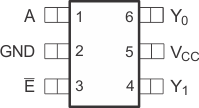
DCK Package
6-Pin SC70
Top View

DRL Package
6-Pin SOT-5X3
Top View

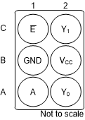
YZP Package
6-Pin DSBGA
Bottom View

See mechanical drawings for dimensions.
Pin Functions
| PIN | I/O | DESCRIPTION | ||
|---|---|---|---|---|
| NAME | DBV, DCK, DRL | YZP | ||
| A | 1 | A1 | I | A Input |
| E | 3 | C1 | I | Active Low Enable |
| GND | 2 | B1 | — | Ground |
| VCC | 5 | B2 | — | Positive Supply |
| Y0 | 6 | A2 | O | Y0 True Output |
| Y1 | 4 | C2 | O | Y1 Complemented Output |