SCES590E JULY 2004 – March 2018 SN74AUP1G06
PRODUCTION DATA.
- 1 Features
- 2 Applications
- 3 Description
- 4 Revision History
- 5 Pin Functions and Configurations
-
6 Specifications
- 6.1 Absolute Maximum Ratings
- 6.2 ESD Ratings
- 6.3 Recommended Operating Conditions
- 6.4 Thermal Information
- 6.5 Electrical Characteristics
- 6.6 Switching Characteristics, CL = 5 pF
- 6.7 Switching Characteristics, CL = 10 pF
- 6.8 Switching Characteristics, CL = 15 pF
- 6.9 Switching Characteristics
- 6.10 Operating Characteristics
- 6.11 Typical Characteristics
- 7 Parameter Measurement Information
- 8 Detailed Description
- 9 Application and Implementation
- 10Power Supply Recommendations
- 11Layout
- 12Device and Documentation Support
- 13Mechanical, Packaging, and Orderable Information
封装选项
请参考 PDF 数据表获取器件具体的封装图。
机械数据 (封装 | 引脚)
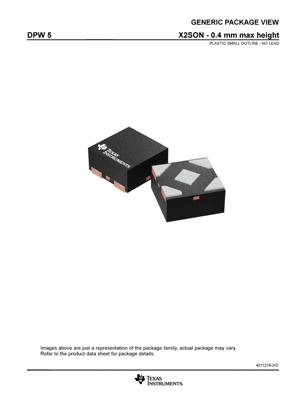
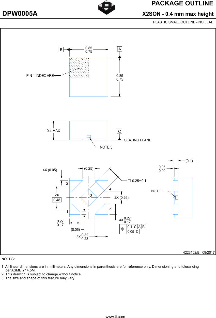
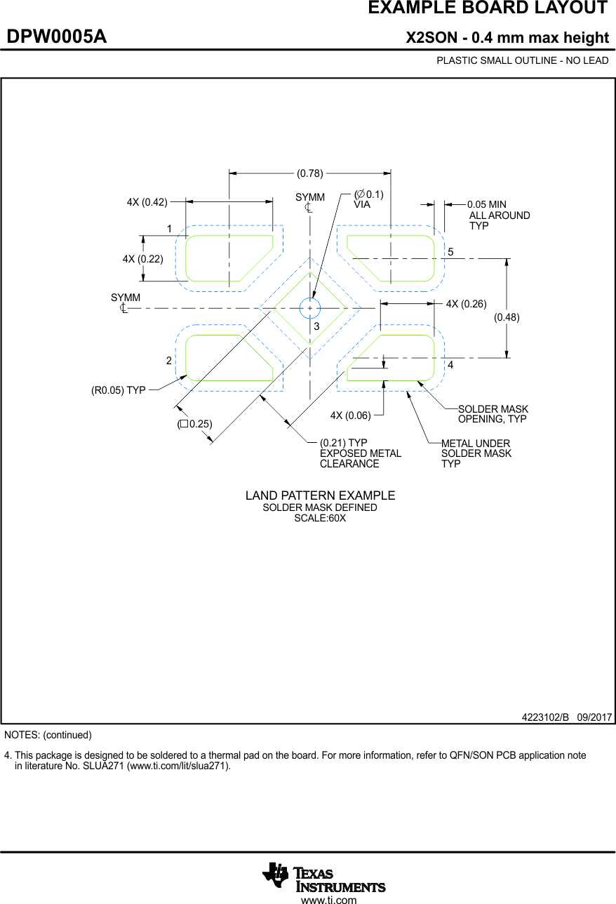
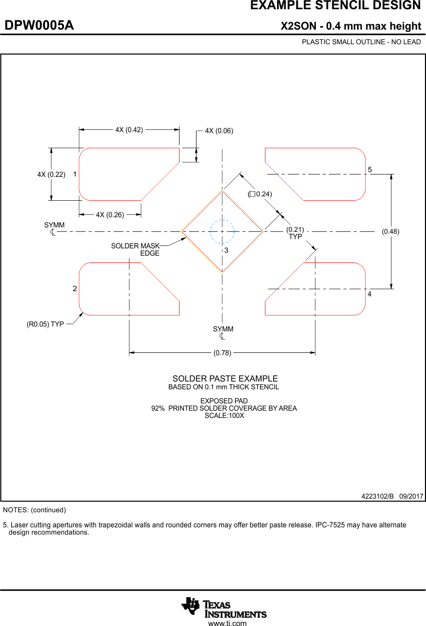
- DPW|5
- DBV|5
- DSF|6
- DCK|5
- DRL|5
- YFP|4
- DRY|6
散热焊盘机械数据 (封装 | 引脚)
- DRY|6
订购信息
13 Mechanical, Packaging, and Orderable Information
The following pages include mechanical, packaging, and orderable information. This information is the most current data available for the designated devices. This data is subject to change without notice and revision of this document. For browser-based versions of this data sheet, refer to the left-hand navigation.


