SCES590E JULY   2004  – March 2018 SN74AUP1G06

PRODUCTION DATA.  

  1. Features
  2. Applications
  3. Description
    1.     Device Images
      1.      Logic Diagram
  4. Revision History
  5. Pin Functions and Configurations
    1.     Pin Functions
  6. Specifications
    1. 6.1  Absolute Maximum Ratings
    2. 6.2  ESD Ratings
    3. 6.3  Recommended Operating Conditions
    4. 6.4  Thermal Information
    5. 6.5  Electrical Characteristics
    6. 6.6  Switching Characteristics, CL = 5 pF
    7. 6.7  Switching Characteristics, CL = 10 pF
    8. 6.8  Switching Characteristics, CL = 15 pF
    9. 6.9  Switching Characteristics
    10. 6.10 Operating Characteristics
    11. 6.11 Typical Characteristics
  7. Parameter Measurement Information
  8. Detailed Description
    1. 8.1 Overview
    2. 8.2 Functional Block Diagram
    3. 8.3 Feature Description
      1. 8.3.1 CMOS Open-Drain Outputs
      2. 8.3.2 Standard CMOS Inputs
      3. 8.3.3 Clamp Diodes
      4. 8.3.4 Partial Power Down (Ioff)
      5. 8.3.5 Over-voltage Tolerant Inputs
    4. 8.4 Device Functional Modes
  9. Application and Implementation
    1. 9.1 Application Information
    2. 9.2 Typical Application
      1. 9.2.1 Design Requirements
      2. 9.2.2 Detailed Design Procedure
      3. 9.2.3 Application Curve
  10. 10Power Supply Recommendations
  11. 11Layout
    1. 11.1 Layout Guidelines
    2. 11.2 Layout Example
  12. 12Device and Documentation Support
    1. 12.1 Documentation Support
      1. 12.1.1 Related Documentation
    2. 12.2 Receiving Notification of Documentation Updates
    3. 12.3 Community Resources
    4. 12.4 Trademarks
    5. 12.5 Electrostatic Discharge Caution
    6. 12.6 Glossary
  13. 13Mechanical, Packaging, and Orderable Information

封装选项

请参考 PDF 数据表获取器件具体的封装图。

机械数据 (封装 | 引脚)
  • DPW|5
  • DBV|5
  • DSF|6
  • DCK|5
  • DRL|5
  • YFP|4
  • DRY|6
散热焊盘机械数据 (封装 | 引脚)
订购信息

Pin Functions and Configurations

DBV Package
5-Pin SOT-23
Top View
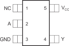
SN74AUP1G06 dbv_package_top_view_ces590.gif
See mechanical drawings for dimensions.
NC – No internal connection
DCK Package
5-Pin SC70
Top View
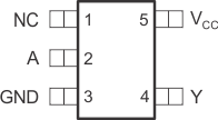
SN74AUP1G06 dck_package_top_view_ces590.gif
DRL Package
5-Pin SOT-5X3
Top View
SN74AUP1G06 po_sces590.gif
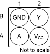
YFP Package
4-Pin DSBGA
Bottom View
SN74AUP1G06 SN74AUP1G06-yfp-package-pinout.gif
DRY Package
6-Pin SON
Top View
SN74AUP1G06 dry_package_top_view_ces590.gif
DSF Package
6-Pin SON
Top View
SN74AUP1G06 dsf_package_top_view_ces590.gif
DPW Package(1)
5-Pin X2SON
Top View
SN74AUP1G06 DPW_Pinout.gif

Pin Functions

PIN(2) I/O DESCRIPTION
NAME DBV, DCK, DRL, DPW DRY, DSF YFP
A 2 2 A1 I Input
GND 3 3 B1 Ground
NC(1) 1 1, 5 Not connected
VCC 5 6 A2 Positive supply
Y 4 4 B2 O Output
NC – No internal connection
See mechanical drawings for dimensions