SCES596G JULY 2004 – August 2017 SN74AUP1G126
PRODUCTION DATA.
- 1 Features
- 2 Applications
- 3 Description
- 4 Revision History
- 5 Pin Configuration and Functions
-
6 Specifications
- 6.1 Absolute Maximum Ratings
- 6.2 ESD Ratings
- 6.3 Recommended Operating Conditions
- 6.4 Thermal Information
- 6.5 Electrical Characteristics
- 6.6 Switching Characteristics: CL = 5 pF
- 6.7 Switching Characteristics: CL = 10 pF
- 6.8 Switching Characteristics: CL = 15 pF
- 6.9 Switching Characteristics: CL = 30 pF
- 6.10 Operating Characteristics
- 6.11 Typical Characteristics
- 7 Parameter Measurement Information
- 8 Detailed Description
- 9 Application and Implementation
- 10Power Supply Recommendations
- 11Layout
- 12Device and Documentation Support
- 13Mechanical, Packaging, and Orderable Information
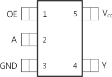
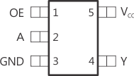
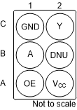
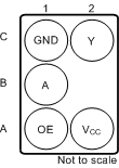
5 Pin Configuration and Functions
DBV Package
5-Pin SOT-23
Top View

DKC Package
5-Pin SOT-23
Top View

DRL Package
5-Pin SOT-5X3
Top View

DPW Package
5-Pin X2SON
Top View

DRY Package
6-Pin SON
Top View

N.C. – No internal connection.
See mechanical drawings for dimensions.
DSF Package
6-Pin SON
Top View

YFP Package
6-Pin DSBGA
Bottom View

YZP Package
5-Pin DSBGA
Bottom View

Pin Functions
| PIN | I/O | DESCRIPTION | ||||
|---|---|---|---|---|---|---|
| NAME | DBV, DCK, DRL, DPW | DRY, DSF | YFP | YZP | ||
| A | 2 | 2 | B1 | B1 | I | Input |
| DNU | — | — | — | B2 | — | Do not use |
| GND | 3 | 3 | C1 | C1 | — | Ground |
| N.C. | — | 5 | B2 | — | — | No Internal Connection |
| OE | 1 | 1 | A1 | A1 | I | Output enable (active high) |
| VCC | 5 | 6 | A2 | A2 | — | Positive supply |
| Y | 4 | 4 | C2 | C2 | O | Buffered output |