SCES579J JUNE 2004 – September 2017 SN74AUP1G17
PRODUCTION DATA.
- 1 Features
- 2 Applications
- 3 Description
- 4 Revision History
- 5 Pin Configuration and Functions
-
6 Specifications
- 6.1 Absolute Maximum Ratings
- 6.2 ESD Ratings
- 6.3 Recommended Operating Conditions
- 6.4 Thermal Information
- 6.5 Electrical Characteristics
- 6.6 Switching Characteristics: CL = 5 pF
- 6.7 Switching Characteristics: CL = 10 pF
- 6.8 Switching Characteristics: CL = 15 pF
- 6.9 Switching Characteristics: CL = 30 pF
- 6.10 Operating Characteristics
- 6.11 Typical Characteristics
- 7 Parameter Measurement Information
- 8 Detailed Description
- 9 Application and Implementation
- 10Power Supply Recommendations
- 11Layout
- 12Device and Documentation Support
- 13Mechanical, Packaging, and Orderable Information
11 Layout
11.1 Layout Guidelines
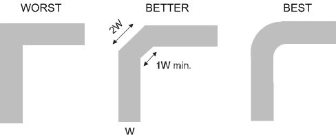
Even low data rate digital signals can contain high-frequency signal components due to fast edge rates. When a printed-circuit board (PCB) trace turns a corner at a 90° angle, a reflection can occur. A reflection occurs primarily because of the change of width of the trace. At the apex of the turn, the trace width increases to 1.414 times the width. This increase upsets the transmission-line characteristics, especially the distributed capacitance and self–inductance of the trace which results in the reflection. Not all PCB traces can be straight and therefore some traces must turn corners. Figure 10 shows progressively better techniques of rounding corners. Only the last example (BEST) maintains constant trace width and minimizes reflections.
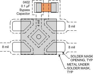
An example layout is given in Figure 11 for the DPW (X2SON-5) package. This example layout includes a 0402 (metric) capacitor and uses the measurements found in the example board layout appended to this end of this datasheet. A via of diameter 0.1 mm (3.973 mil) is placed directly in the center of the device. This via can be used to trace out the center pin connection through another board layer, or it can be left out of the layout
11.2 Layout Example
 Figure 10. Trace Example
 Figure 11. Example Layout With DPW (X2SON-5) Package