SCES627D MARCH 2005 – October 2017 SN74AUP1G240
PRODUCTION DATA.
- 1 Features
- 2 Applications
- 3 Description
- 4 Revision History
- 5 Pin Configuration and Functions
-
6 Specifications
- 6.1 Absolute Maximum Ratings
- 6.2 ESD Ratings
- 6.3 Recommended Operating Conditions
- 6.4 Thermal Information
- 6.5 Electrical Characteristics
- 6.6 Switching Characteristics: CL = 5 pF
- 6.7 Switching Characteristics: CL = 10 pF
- 6.8 Switching Characteristics: CL = 15 pF
- 6.9 Switching Characteristics: CL = 30 pF
- 6.10 Operating Characteristics
- 6.11 Typical Characteristics
- 7 Parameter Measurement Information
- 8 Detailed Description
- 9 Application and Implementation
- 10Power Supply Recommendations
- 11Layout
- 12Device and Documentation Support
- 13Mechanical, Packaging, and Orderable Information
封装选项
机械数据 (封装 | 引脚)
散热焊盘机械数据 (封装 | 引脚)
订购信息
8 Detailed Description
8.1 Overview
The SN74AUP1G240 device contains one inverter gate device with active low output enable control and performs the Boolean function Y = A. This device is fully specified for partial-power-down applications using Ioff. The Ioff circuitry disables the outputs when the device is powered down. This inhibits current backflow into the device, which prevents damage to the device. To assure the high-impedance state during power up or power down, OE must be tied to VCC through a pullup resistor; the minimum value of the resistor is determined by the current-sinking capability of the driver.
8.2 Functional Block Diagram
 Figure 4. Logic Diagram (Positive Logic)
8.3 Feature Description
8.3.1 Balanced 3-State High-Drive CMOS Push-Pull Outputs
A balanced output allows the device to sink and source similar currents. The high drive capability of this device creates fast edges into light loads so routing and load conditions should be considered to prevent ringing. Additionally, the outputs of this device are capable of driving larger currents than the device can sustain without being damaged. It is important for the power output of the device to be limited to avoid thermal runaway and damage due to over-current. The electrical and thermal limits defined the in the Absolute Maximum Ratings table must be followed at all times.
3-State outputs can be put into a high-impedance mode, in which the device will neither source nor sink current.
8.3.2 Standard CMOS Inputs
Standard CMOS inputs are high impedance and are typically modelled as a resistor in parallel with the input capacitance given in the Electrical Characteristics table. The worst case resistance is calculated with the maximum input voltage, given in the Absolute Maximum Ratings table, and the maximum input leakage current, given in the Electrical Characteristics table, using ohm's law (R = V ÷ I).
Signals applied to the inputs need to have fast edge rates, as defined by Δt/Δv in the Recommended Operating Conditions table to avoid excessive currents and oscillations. If a slow or noisy input signal is required, a device with a Schmitt-trigger input should be utilized to condition the input signal prior to the standard CMOS input.
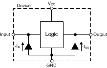
8.3.3 Clamp Diodes
The inputs and outputs to this device have negative clamping diodes.
CAUTION
Voltages beyond the values specified in the Absolute Maximum Ratings table can cause damage to the device. The input negative-voltage and output voltage ratings may be exceeded if the input and output clamp-current ratings are observed.
 Figure 5. Electrical Placement of Clamping Diodes for Each Input and Output
8.3.4 Partial Power Down (Ioff)
The inputs and outputs for this device enter a high impedance state when the supply voltage is 0 V. The maximum leakage into or out of any input or output pin on the device is specified by Ioff in the Electrical Characteristics table.
8.3.5 Over-Voltage Tolerant Inputs
Input signals to this device can be driven above the supply voltage so long as they remain below the maximum input voltage value specified in the Absolute Maximum Ratings table.