SCES503J NOVEMBER 2003 – June 2015 SN74AUP1G57
PRODUCTION DATA.
- 1 Features
- 2 Applications
- 3 Description
- 4 Revision History
- 5 Pin Configuration and Functions
-
6 Specifications
- 6.1 Absolute Maximum Ratings
- 6.2 ESD Ratings
- 6.3 Recommended Operating Conditions
- 6.4 Thermal Information
- 6.5 Electrical Characteristics
- 6.6 Switching Characteristics, CL = 5 pF
- 6.7 Switching Characteristics, CL = 10 pF
- 6.8 Switching Characteristics, CL = 15 pF
- 6.9 Switching Characteristics, CL = 30 pF
- 6.10 Operating Characteristics
- 6.11 Typical Characteristics
- 7 Parameter Measurement Information
- 8 Detailed Description
- 9 Application and Implementation
- 10Power Supply Recommendations
- 11Layout
- 12Device and Documentation Support
- 13Mechanical, Packaging, and Orderable Information
封装选项
机械数据 (封装 | 引脚)
散热焊盘机械数据 (封装 | 引脚)
- DRY|6
订购信息
8 Detailed Description
8.1 Overview
The AUP family is TI's premier solution to the low-power needs of the industry in battery-powered portable applications. This family ensures a very low static and dynamic power consumption across the entire VCC range of 0.8 V to 3.6 V, resulting in an increased battery life. This product also maintains excellent signal integrity, which produces very low undershoot and overshoot characteristics.
The SN74AUP1G57 features configurable multiple functions. The output state is determined by eight patterns of 3-bit input. The user can choose the logic functions AND, OR, NAND, NOR, XNOR, inverter, and noninverter. All inputs can be connected to VCC or GND.
The device functions as an independent gate with Schmitt-trigger inputs, which allow for slow input transition and better switching noise immunity at the input.
NanoStar package technology is a major breakthrough in IC packaging concepts, using the die as the package.
This device is fully specified for partial-power-down applications using Ioff. The Ioff circuitry disables the outputs, preventing damaging current backflow through the device when it is powered down.
8.2 Functional Block Diagram

8.3 Feature Description
This part is available in the TI NanoStar package. It has low static-power consumption with ICC = 0.9 μA maximum and low dynamic power consumption (Cpd = 4.3 pF, Typical at 3.3 V).
The inputs have low capacitance, with typical Ci = 1.5 pF.
This part has low noise, with overshoot and undershoot less than 10% of VCC.
This part supports partial-power-down mode operation. When this part is powered down (VCC = 0 V), the leakage current into the device is characterized by Ioff.
Schmitt-trigger inputs provide hysterisis and consistency in VIH / VIL.
It has a wide operating VCC range of 0.8 V to 3.6 V, and has been optimized for 3.3-V operation.
3.6-V I/O tolerant to support mixed-mode signal operation.
It has a low propagation delay of 5.3 ns at 3.3 V.
It is suitable for point-to-point applications.
8.4 Device Functional Modes
Table 1 lists all the functional modes of the SN74AUP1G57.
Table 1. Function Table
| INPUTS | OUTPUT Y |
||
|---|---|---|---|
| In2 | In1 | In0 | |
| L | L | L | H |
| L | L | H | L |
| L | H | L | H |
| L | H | H | L |
| H | L | L | L |
| H | L | H | L |
| H | H | L | H |
| H | H | H | H |
8.4.1 Logic Configurations
Table 2 lists all the logic functions of the SN74AUP1G57.
Table 2. Function Selection Table
| LOGIC FUNCTION | FIGURE NO. |
|---|---|
| 2-input AND | Figure 4 |
| 2-input AND with both inputs inverted | Figure 7 |
| 2-input NAND with inverted input | Figure 5, Figure 6 |
| 2-input OR with inverted input | Figure 5, Figure 6 |
| 2-input NOR | Figure 7 |
| 2-input NOR with both inputs inverted | Figure 4 |
| 2-input XNOR | Figure 8 |
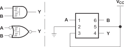 Figure 4. 2-Input AND Gate
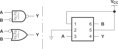 Figure 6. 2-Input NAND Gate With Inverted B Input
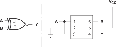 Figure 8. 2-Input XNOR Gate
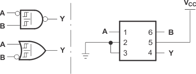 Figure 5. 2-Input NAND Gate With Inverted A Input
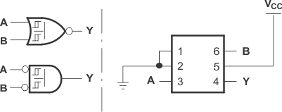 Figure 7. 2-Input NOR Gate