SCES592I July 2004 – September 2017 SN74AUP1G79
PRODUCTION DATA.
- 1 Features
- 2 Applications
- 3 Description
- 4 Revision History
- 5 Pin Configuration and Functions
-
6 Specifications
- 6.1 Absolute Maximum Ratings
- 6.2 ESD Ratings
- 6.3 Recommended Operating Conditions
- 6.4 Thermal Information
- 6.5 Electrical Characteristics: TA = 25°C
- 6.6 Electrical Characteristics: TA = -40°C to 85°C
- 6.7 Timing Requirements
- 6.8 Switching Characteristics: CL = 5 pF
- 6.9 Switching Characteristics: CL = 10 pF
- 6.10 Switching Characteristics: CL = 15 pF
- 6.11 Switching Characteristics: CL = 30 pF
- 6.12 Operating Characteristics
- 6.13 Typical Characteristics
- 7 Parameter Measurement Information
- 8 Detailed Description
- 9 Applications, Implementation, and Layout
- 10Power Supply Recommendations
- 11Layout
- 12Device and Documentation Support
- 13Mechanical, Packaging, and Orderable Information
封装选项
机械数据 (封装 | 引脚)
散热焊盘机械数据 (封装 | 引脚)
订购信息
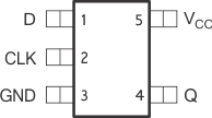
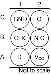
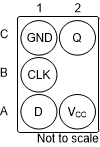
5 Pin Configuration and Functions
DBV Package
5-Pin SOT-23
Top View

DCK Package
5-Pin SC70
Top View

DRL Package
5-Pin SOT-5X3
Top View

DPW Package
5-Pin X2SON
Top View

DRY Package
6-Pin SON
Top View

DSF Package
6-Pin SON
Top View

YFP Package
6-Pin DSBGA
Bottom View

YZP Package
5-Pin DSBGA
Bottom View

Pin Functions
| PIN | I/O | DESCRIPTION | ||||
|---|---|---|---|---|---|---|
| NAME | DBV, DCK, DRL, DPW |
DRY, DSF |
YZP | YFP | ||
| CLK | 2 | 2 | B1 | B1 | I | Positive-Edge-Triggered Clock input |
| D | 1 | 1 | A1 | A1 | I | Data Input |
| GND | 3 | 3 | C1 | C1 | — | Ground pin |
| NC | — | 5 | — | B2 | — | No Connect |
| Q | 4 | 4 | C2 | C2 | O | Q output |
| VCC | 5 | 6 | A2 | A2 | — | Positive supply |