SCES593F JULY 2004 – July 2017 SN74AUP1G80
PRODUCTION DATA.
- 1 Features
- 2 Applications
- 3 Description
- 4 Revision History
- 5 Pin Configuration and Functions
-
6 Specifications
- 6.1 Absolute Maximum Ratings
- 6.2 ESD Ratings
- 6.3 Recommended Operating Conditions
- 6.4 Thermal Information
- 6.5 Electrical Characteristics: TA = 25°C
- 6.6 Electrical Characteristics: TA = -40°C to +85°C
- 6.7 Timing Requirements
- 6.8 Switching Characteristics: CL = 5 pF
- 6.9 Switching Characteristics: CL = 10 pF
- 6.10 Switching Characteristics: CL = 15 pF
- 6.11 Switching Characteristics: CL = 30 pF
- 6.12 Operating Characteristics
- 6.13 Typical Characteristics
- 7 Parameter Measurement Information
- 8 Detailed Description
- 9 Application and Implementation
- 10Power Supply Recommendations
- 11Layout
- 12Device and Documentation Support
- 13Mechanical, Packaging, and Orderable Information
封装选项
机械数据 (封装 | 引脚)
散热焊盘机械数据 (封装 | 引脚)
订购信息
9 Application and Implementation
NOTE
Information in the following applications sections is not part of the TI component specification, and TI does not warrant its accuracy or completeness. TI’s customers are responsible for determining suitability of components for their purposes. Customers should validate and test their design implementation to confirm system functionality.
9.1 Application Information
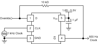
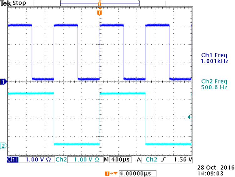
A useful application for the SN74AUP1G80 is using it as a frequency divider. By feeding back the output (Q) to the input (D), the output toggles on every rising edge of the clock waveform. The output goes HIGH once every two clock cycles, so essentially the frequency of the clock signal is divided by a factor of two. The device does not have preset or clear functions so the initial state of the output is unknown. This application implements the use of an override pin to initially set the input HIGH or LOW. Initialization is not needed, but should be kept in mind. Post initialization, the Override input is set to a high-impedance mode, or it can be used to force a HIGH or LOW output.
9.2 Typical Application
 Figure 7. Clock Frequency Division
9.2.1 Design Requirements
For this application, a resistor must be placed on the feedback line in order for the initialization voltage from the override input to overpower the signal coming from the output (Q). Without a resistor the state at the input would be unknown as the output of the SN74AUP1G80 is driving the line separate from the Override input.
The SN74AUP1G80 device uses CMOS technology and has balanced output drive. Take care to avoid bus contention because it can drive currents that would exceed maximum limits.
9.2.2 Detailed Design Procedure
- Recommended input conditions:
- For rise time and fall time specifications, see Δt/Δv in the Recommended Operating Conditions table.
- For specified high and low levels, see VIH and VIL in the Recommended Operating Conditions table.
- Input voltages are recommended to not go below 0 V and not exceed 4.6 V for any VCC. See the Absolute Maximum Ratings table.
- Recommended output conditions:
- Load currents should not exceed ±20 mA. See the Absolute Maximum Ratings table.
- Output voltages are recommended to not go below 0 V and not exceed the VCC voltage. See the Absolute Maximum Ratings table.
- Feedback resistor:
- A 10-kΩ resistor is chosen to bias the input so the Override input can initialize the input and output. The resistor value is important because a resistance too high, such as 1 MΩ, would cause too much of a voltage drop, causing the output to no longer be able to drive the input. On the other hand, a resistor too low, such as a 1 Ω, would not bias enough and might cause bus contention between the Q output and the override input, possibly damaging the device.
9.2.3 Application Curve
 Figure 8. Frequency Division