SCES803A April 2010 – June 2015 SN74AUP1T17
PRODUCTION DATA.
- 1 Features
- 2 Applications
- 3 Description
- 4 Revision History
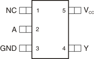
- 5 Pin Configuration and Functions
-
6 Specifications
- 6.1 Absolute Maximum Ratings
- 6.2 ESD Ratings
- 6.3 Recommended Operating Conditions
- 6.4 Thermal Information
- 6.5 Electrical Characteristics
- 6.6 Switching Characteristics, VCC = 2.5 V and VI = 1.8 V
- 6.7 Switching Characteristics, VCC = 2.5 V and VI = 2.5 V
- 6.8 Switching Characteristics, VCC = 2.5 V and VI = 3.3 V
- 6.9 Switching Characteristics, VCC = 3.3 V and VI = 1.8 V
- 6.10 Switching Characteristics, VCC = 3.3 V and VI = 2.5 V
- 6.11 Switching Characteristics, VCC = 3.3 V and VI = 3.3 V
- 6.12 Operating Characteristics
- 6.13 Typical Characteristics
- 7 Parameter Measurement Information
- 8 Detailed Description
- 9 Application and Implementation
- 10Power Supply Recommendations
- 11Layout
- 12Device and Documentation Support
- 13Mechanical, Packaging, and Orderable Information
