ZHCSEZ0A December   2013  – April 2016 SN74AUP1T34-Q1

PRODUCTION DATA.  

  1. 特性
  2. 应用范围
  3. 说明
  4. 修订历史记录
  5. Pin Configuration and Functions
  6. Specifications
    1. 6.1 Absolute Maximum Ratings
    2. 6.2 ESD Ratings
    3. 6.3 Recommended Operating Conditions
    4. 6.4 Thermal Information
    5. 6.5 AC Electrical Characteristics
    6. 6.6 Typical Characteristics
  7. Parameter Measurement Information
  8. Detailed Description
    1. 8.1 Overview
    2. 8.2 Functional Block Diagram
    3. 8.3 Feature Description
      1. 8.3.1 Fully Configurable Dual-Rail Design
      2. 8.3.2 Partial-Power-Down Mode Operation
      3. 8.3.3 VCC Isolation
      4. 8.3.4 Input Hysteresis
    4. 8.4 Device Functional Modes
  9. Application and Implementation
    1. 9.1 Application Information
    2. 9.2 Typical Application
      1. 9.2.1 Design Requirements
      2. 9.2.2 Detailed Design Procedure
      3. 9.2.3 Application Curve
  10. 10Power Supply Recommendations
  11. 11Layout
    1. 11.1 Layout Guidelines
    2. 11.2 Layout Example
  12. 12器件和文档支持
    1. 12.1 社区资源
    2. 12.2 商标
    3. 12.3 静电放电警告
    4. 12.4 Glossary
  13. 13机械、封装和可订购信息

封装选项

机械数据 (封装 | 引脚)
散热焊盘机械数据 (封装 | 引脚)
订购信息

11 Layout

11.1 Layout Guidelines

To ensure reliability of the device, TI recommends following common printed-circuit board layout guidelines.

  • Bypass capacitors must be used on power supplies.
  • Short trace lengths must be used to avoid excessive loading.
  • Placing pads on the signal paths for loading capacitors or pullup resistors helps adjust rise and fall times of signals depending on the system requirements.

11.2 Layout Example
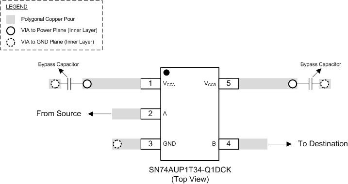
SN74AUP1T34-Q1 SN74AUP1T34-Q1_Layout_Example.gif Figure 6. Example Layout