ZHCSTY0E December 2008 – November 2023 SN74AVC8T245-Q1
PRODUCTION DATA
- 1
- 1 特性
- 2 应用
- 3 说明
- 4 Pin Configuration and Functions
-
5 Specifications
- 5.1 Absolute Maximum Ratings
- 5.2 ESD Ratings
- 5.3 Recommended Operating Conditions
- 5.4 Thermal Information
- 5.5 Electrical Characteristics
- 5.6 Switching Characteristics: VCCA = 1.2 V
- 5.7 Switching Characteristics: VCCA = 1.5 V ± 0.1 V
- 5.8 Switching Characteristics: VCCA = 1.8 V ± 0.15 V
- 5.9 Switching Characteristics: VCCA = 2.5 V ± 0.2 V
- 5.10 Switching Characteristics: VCCA = 3.3 V ± 0.3 V
- 5.11 Operating Characteristics
- 5.12 Typical Total Static Current Consumption (ICCA + ICCB)
- 5.13 Typical Characteristics
- 6 Parameter Measurement Information
- 7 Detailed Description
- 8 Application and Implementation
- 9 Device and Documentation Support
- 10Revision History
- 11Mechanical, Packaging, and Orderable Information
4 Pin Configuration and Functions
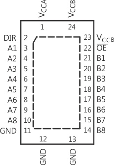
 Figure 4-1 RHL Package, 24-Pin VQFN
(Top View)
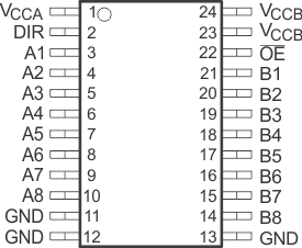
 Figure 4-2 PW Package, 24-Pin TSSOP
(Top View)
Figure 4-2 PW Package, 24-Pin TSSOP
(Top View)Table 4-1 Pin Functions
| PIN | TYPE(1) | DESCRIPTION | |||
|---|---|---|---|---|---|
| NAME | VQFN | TSSOP | |||
| A1 | 3 | 3 | I/O | Input/output A1. Referenced to VCCA. | |
| A2 | 4 | 4 | I/O | Input/output A2. Referenced to VCCA. | |
| A3 | 5 | 5 | I/O | Input/output A3. Referenced to VCCA. | |
| A4 | 6 | 6 | I/O | Input/output A4. Referenced to VCCA. | |
| A5 | 7 | 7 | I/O | Input/output A5. Referenced to VCCA. | |
| A6 | 8 | 8 | I/O | Input/output A6. Referenced to VCCA. | |
| A7 | 9 | 9 | I/O | Input/output A7. Referenced to VCCA. | |
| A8 | 10 | 10 | I/O | Input/output A8. Referenced to VCCA. | |
| B1 | 21 | 21 | I/O | Input/output B1. Referenced to VCCB. | |
| B2 | 20 | 20 | I/O | Input/output B2. Referenced to VCCB. | |
| B3 | 19 | 19 | I/O | Input/output B3. Referenced to VCCB. | |
| B4 | 18 | 18 | I/O | Input/output B4. Referenced to VCCB. | |
| B5 | 17 | 17 | I/O | Input/output B5. Referenced to VCCB. | |
| B6 | 16 | 16 | I/O | Input/output B6. Referenced to VCCB. | |
| B7 | 15 | 15 | I/O | Input/output B7. Referenced to VCCB. | |
| B8 | 14 | 14 | I/O | Input/output B8. Referenced to VCCB. | |
| DIR | 2 | — | I | Direction-control input for 1 ports | |
| GND | 12, 13 | 11, 12, 13 | — | Ground | |
| OE | 22 | 22 | I | 3-state output-mode enable. Pull OE high to place ‘2’ outputs in 3-state mode. Referenced to VCCA. | |
| VCCA | 1 | 1 | — | A-port power supply voltage. 1.2 V ≤ VCCA ≤ 3.6 V | |
| VCCB | 23, 24 | 23, 24 | — | B-port power supply voltage. 1.2 V ≤ VCCB ≤ 3.6 V | |
| Thermal pad | — | The exposed thermal pad must be connected as a secondary GND or be left electrically open. | |||
(1) I = input, O = output