ZHCSJI7 March 2019 SN74AXCH4T245
PRODUCTION DATA.
- 1 特性
- 2 应用
- 3 说明
- 4 修订历史记录
- 5 Pin Configuration and Functions
-
6 Specifications
- 6.1 Absolute Maximum Ratings
- 6.2 ESD Ratings
- 6.3 Recommended Operating Conditions
- 6.4 Thermal Information
- 6.5 Electrical Characteristics
- 6.6 Switching Characteristics, VCCA = 0.7 ± 0.05 V
- 6.7 Switching Characteristics, VCCA = 0.8 ± 0.04 V
- 6.8 Switching Characteristics, VCCA = 0.9 ± 0.045 V
- 6.9 Switching Characteristics, VCCA = 1.2 ± 0.1 V
- 6.10 Switching Characteristics, VCCA = 1.5 ± 0.1 V
- 6.11 Switching Characteristics, VCCA = 1.8 ± 0.15 V
- 6.12 Switching Characteristics, VCCA = 2.5 ± 0.2 V
- 6.13 Switching Characteristics, VCCA = 3.3 ± 0.3 V
- 6.14 Operating Characteristics: TA = 25°C
- 6.15 Typical Characteristics
- 7 Parameter Measurement Information
-
8 Detailed Description
- 8.1 Overview
- 8.2 Functional Block Diagram
- 8.3
Feature Description
- 8.3.1 Standard CMOS Inputs
- 8.3.2 Balanced High-Drive CMOS Push-Pull Outputs
- 8.3.3 Partial Power Down (Ioff)
- 8.3.4 VCC Isolation
- 8.3.5 Over-voltage Tolerant Inputs
- 8.3.6 Glitch-free Power Supply Sequencing
- 8.3.7 Negative Clamping Diodes
- 8.3.8 Fully Configurable Dual-Rail Design
- 8.3.9 Supports High-Speed Translation
- 8.3.10 Bus-Hold Data Inputs
- 8.4 Device Functional Modes
- 9 Application and Implementation
- 10Power Supply Recommendations
- 11Layout
- 12器件和文档支持
- 13机械、封装和可订购信息
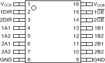
5 Pin Configuration and Functions
PW Package
16-Pin TSSOP
Top View

RSV Package
16-Pin UQFN
Transparent Top View

Pin Functions
| PIN | NO. | TYPE | DESCRIPTION | ||
|---|---|---|---|---|---|
| NAME | PW | RSV | |||
| 1A1 | 4 | 6 | I/O | Input/output 1A1. Referenced to VCCA. | |
| 1A2 | 5 | 7 | I/O | Input/output 1A2. Referenced to VCCA. | |
| 1B1 | 13 | 15 | I/O | Input/output 1B1. Referenced to VCCB. | |
| 1B2 | 12 | 14 | I/O | Input/output 1B2. Referenced to VCCB. | |
| 1DIR | 2 | 4 | I | Direction-control input for ‘1’ ports | |
| 1OE | 15 | 1 | I | Tri-state output-mode enable. Pull OE high to place ‘1’ outputs in tri-state mode. Referenced to VCCA. | |
| 2A1 | 6 | 8 | I/O | Input/output 2A1. Referenced to VCCA. | |
| 2A2 | 7 | 9 | I/O | Input/output 2A2. Referenced to VCCA. | |
| 2B1 | 11 | 13 | I/O | Input/output 2B1. Referenced to VCCB. | |
| 2B2 | 10 | 12 | I/O | Input/output 2B2. Referenced to VCCB. | |
| 2DIR | 3 | 5 | I | Direction-control input for ‘2’ ports | |
| 2OE | 14 | 16 | I | Tri-state output-mode enable. Pull OE high to place ‘2’ outputs in tri-state mode. Referenced to VCCA. | |
| GND | 8, 9 | 10, 11 | — | Ground | |
| VCCA | 1 | 3 | — | A-port power supply voltage. 0.65 V ≤ VCCA ≤ 3.6 V | |
| VCCB | 16 | 2 | — | B-port power supply voltage. 0.65 V ≤ VCCB ≤ 3.6 V | |