ZHCSIL3A August 2018 – January 2019 SN74AXCH8T245
PRODUCTION DATA.
- 1 特性
- 2 应用
- 3 说明
- 4 修订历史记录
- 5 Pin Configuration and Functions
-
6 Specifications
- 6.1 Absolute Maximum Ratings
- 6.2 ESD Ratings
- 6.3 Recommended Operating Conditions
- 6.4 Thermal Information
- 6.5 Electrical Characteristics
- 6.6 Switching Characteristics, VCCA = 0.7 V
- 6.7 Switching Characteristics, VCCA = 0.8 V
- 6.8 Switching Characteristics, VCCA = 0.9 V
- 6.9 Switching Characteristics, VCCA = 1.2 V
- 6.10 Switching Characteristics, VCCA = 1.5 V
- 6.11 Switching Characteristics, VCCA = 1.8 V
- 6.12 Switching Characteristics, VCCA = 2.5 V
- 6.13 Switching Characteristics, VCCA = 3.3 V
- 6.14 Operating Characteristics: TA = 25°C
- 7 Parameter Measurement Information
- 8 Detailed Description
- 9 Application and Implementation
- 10Power Supply Recommendations
- 11Layout
- 12器件和文档支持
- 13机械、封装和可订购信息
5 Pin Configuration and Functions
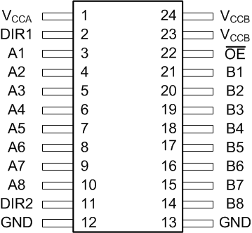
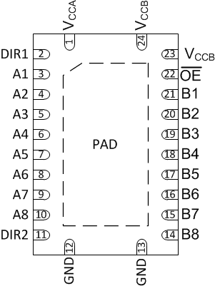
PW Package
24-Pin TSSOP
Top View

Pin Functions
| PIN | I/O | DESCRIPTION | |
|---|---|---|---|
| NAME | PW, RHL | ||
| A1 | 3 | I/O | Input/output A1. Referenced to VCCA. |
| A2 | 4 | I/O | Input/output A2. Referenced to VCCA. |
| A3 | 5 | I/O | Input/output A3. Referenced to VCCA. |
| A4 | 6 | I/O | Input/output A4. Referenced to VCCA. |
| A5 | 7 | I/O | Input/output A5. Referenced to VCCA. |
| A6 | 8 | I/O | Input/output A6. Referenced to VCCA. |
| A7 | 9 | I/O | Input/output A7. Referenced to VCCA. |
| A8 | 10 | I/O | Input/output A8. Referenced to VCCA. |
| B1 | 21 | I/O | Input/output B1. Referenced to VCCB. |
| B2 | 20 | I/O | Input/output B2. Referenced to VCCB. |
| B3 | 19 | I/O | Input/output B3. Referenced to VCCB. |
| B4 | 18 | I/O | Input/output B4. Referenced to VCCB. |
| B5 | 17 | I/O | Input/output B5. Referenced to VCCB. |
| B6 | 16 | I/O | Input/output B6. Referenced to VCCB. |
| B7 | 15 | I/O | Input/output B7. Referenced to VCCB. |
| B8 | 14 | I/O | Input/output B8. Referenced to VCCB. |
| DIR1 | 2 | I | Direction-control signal. Referenced to VCCA. |
| DIR2 | 11 | I | Direction-control signal. Referenced to VCCA. See for additional details. Tie to GND to maintain backwards compatibility with the SN74AVCH8T245 device. |
| GND | 12 | — | Ground |
| 13 | — | Ground | |
| OE | 22 | I | Output Enable. Pull to GND to enable all outputs. Pull to VCCA to place all outputs in high-impedance mode. Referenced to VCCA. |
| VCCA | 1 | — | A-port supply voltage. 0.65 V ≤ VCCA ≤ 3.6 V |
| VCCB | 23 | — | B-port supply voltage. 0.65 V ≤ VCCB ≤ 3.6 V |
| 24 | — | B-port supply voltage. 0.65 V ≤ VCCB ≤ 3.6 V | |
(1) PAD - may be grounded (recommended) or left floating.
