SCDS168A May 2004 – September 2015 SN74CB3Q16244
PRODUCTION DATA.
- 1 Features
- 2 Applications
- 3 Description
- 4 Revision History
- 5 Description continued
- 6 Pin Configuration and Functions
- 7 Specifications
- 8 Parameter Measurement Information
- 9 Detailed Description
- 10Application and Implementation
- 11Power Supply Recommendations
- 12Layout
- 13Device and Documentation Support
- 14Mechanical, Packaging, and Orderable Information
封装选项
请参考 PDF 数据表获取器件具体的封装图。
机械数据 (封装 | 引脚)
- DGG|48
- DL|48
- DGV|48
散热焊盘机械数据 (封装 | 引脚)
订购信息
9 Detailed Description
9.1 Overview
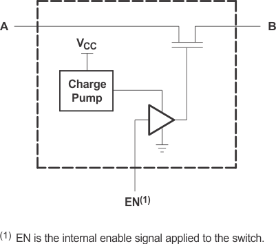
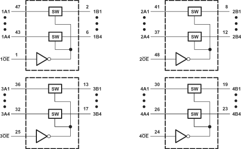
The SN74CB3Q16244 is part of the CB3Q family of switches. The SN74CB3Q16244 is a 16-bit FET bus switch in which 4 Output Enable pins each control a set of 4 switches totaling 16 switches.
 Figure 3. Simplified Schematic, Each FET Switch (SW)
9.2 Functional Block Diagram
 Figure 4. Logic Diagram (Positive Logic)
9.3 Feature Description
The SN74CB3Q16244 device has a high-bandwidth data path (up to 500 MHz) and has 5-V tolerant I/Os with the device powered up or powered down. It also has low and flat ON-state resistance (ron) characteristics over operating range (ron = 5 Ω Typical)
This device also has rail-to-rail switching on data I/O ports for 0 to 5-V switching with 3.3-V VCC and 0 to 3.3-V switching with 2.5-V VCCas well as bidirectional data flow with near-zero propagation delay and low input and output capacitance that minimizes loading and signal distortion (Cio(OFF) = 4 pF Typical)
The SN74CB3Q16244 also provides a fast switching frequency (fOE = 20 MHz Maximum) with data and control inputs that provide undershoot clamp diodes as well as low power consumption (ICC = 1 mA Typical)
The VCC operating range is from 2.3 V to 3.6 V and the data I/Os support 0 to 5-V signal levels of (0.8-V, 1.2-V, 1.5-V, 1.8-V, 2.5-V, 3.3-V, 5-V)
The control inputs can be driven by TTL or 5-V and 3.3-V CMOS outputs, and Ioff supports partial-power-down mode operation.
9.4 Device Functional Modes
Table 1 lists the functional modes of the SN74CB3Q16244.
Table 1. Function Table
(Each Multiplexer/Demultiplexer)
| INPUT | INPUT/OUTPUT | FUNCTION | ||
|---|---|---|---|---|
| OE | A | |||
| L | B | A port = B port | ||
| H | Z | Disconnect | ||