ZHCSIG9D September 2003 – July 2018 SN74CB3Q3257
PRODUCTION DATA.
- 1 特性
- 2 应用
- 3 说明
- 4 修订历史记录
- 5 Pin Configuration and Functions
- 6 Specifications
- 7 Parameter Measurement Information
- 8 Detailed Description
- 9 Application and Implementation
- 10Power Supply Recommendations
- 11Layout
- 12器件和文档支持
- 13机械、封装和可订购信息
封装选项
请参考 PDF 数据表获取器件具体的封装图。
机械数据 (封装 | 引脚)
- PW|16
- DBQ|16
- RGY|16
- DGV|16
散热焊盘机械数据 (封装 | 引脚)
- RGY|16
订购信息
8.1 Overview
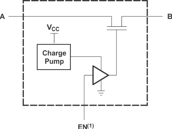
The SN74CB3Q3257 device is a high-bandwidth FET bus switch using a charge pump to elevate the gate voltage of the pass transistor, providing a low and flat ON-state resistance (ron). The low and flat ON-state resistance allows for minimal propagation delay and supports rail-to-rail switching on the data input/output (I/O) ports. The device also features low data I/O capacitance to minimize capacitive loading and signal distortion on the data bus. Specifically designed to support high-bandwidth applications, the SN74CB3Q3257 device provides an optimized interface solution ideally suited for broadband communications, networking, and data-intensive computing systems.
The SN74CB3Q3257 device is organized as two 1-of-4 multiplexers/demultiplexers with separate output-enable (1OE, 2OE) inputs. The select (S0, S1) inputs control the data path of each multiplexer/demultiplexer. When OE is low, the associated multiplexer/demultiplexer is enabled, and the A port is connected to the B port, allowing bidirectional data flow between ports. When OE is high, the associated multiplexer/demultiplexer is disabled, and a high-impedance state exists between the A and B ports.
This device is fully specified for partial-power-down applications using Ioff. The Ioff circuitry prevents damaging current backflow through the device when it is powered down. The device has isolation during power off.
To ensure the high-impedance state during power up or power down, OE should be tied to VCC through a pullup resistor; the minimum value of the resistor is determined by the current-sinking capability of the driver.
