SCLS087F December   1982  – June 2021 SN54HC21 , SN74HC21

PRODUCTION DATA  

  1. Features
  2. Applications
  3. Description
  4. Revision History
  5. Pin Configuration and Functions
    1.     Pin Functions
  6. Specifications
    1. 6.1 Absolute Maximum Ratings
    2. 6.2 Recommended Operating Conditions
    3. 6.3 Thermal Information
    4. 6.4 Electrical Characteristics - 74
    5. 6.5 Electrical Characteristics - 54
    6. 6.6 Switching Characteristics - 74
    7. 6.7 Switching Characteristics - 54
    8. 6.8 Operating Characteristics
    9. 6.9 Typical Characteristics
  7. Parameter Measurement Information
  8. Detailed Description
    1. 8.1 Overview
    2. 8.2 Functional Block Diagram
    3. 8.3 Feature Description
      1. 8.3.1 Balanced CMOS Push-Pull Outputs
      2. 8.3.2 Standard CMOS Inputs
      3. 8.3.3 Clamp Diode Structure
    4. 8.4 Device Functional Modes
  9. Application and Implementation
    1. 9.1 Application Information
    2. 9.2 Typical Application
      1. 9.2.1 Design Requirements
        1. 9.2.1.1 Power Considerations
        2. 9.2.1.2 Input Considerations
        3. 9.2.1.3 Output Considerations
      2. 9.2.2 Detailed Design Procedure
      3. 9.2.3 Application Curves
  10. 10Power Supply Recommendations
  11. 11Layout
    1. 11.1 Layout Guidelines
    2. 11.2 Layout Example
  12. 12Device and Documentation Support
    1. 12.1 Documentation Support
      1. 12.1.1 Related Documentation
    2. 12.2 Support Resources
    3. 12.3 Trademarks
    4. 12.4 Electrostatic Discharge Caution
    5. 12.5 Glossary
  13. 13Mechanical, Packaging, and Orderable Information

封装选项

请参考 PDF 数据表获取器件具体的封装图。

机械数据 (封装 | 引脚)
  • D|14
  • PW|14
  • N|14
  • NS|14
散热焊盘机械数据 (封装 | 引脚)
订购信息

Clamp Diode Structure

The inputs and outputs to this device have both positive and negative clamping diodes as depicted in Figure 8-1.

CAUTION:

Voltages beyond the values specified in the Section 6.1 table can cause damage to the device. The recommended input and output voltage ratings may be exceeded if the input and output clamp-current ratings are observed.
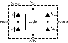
GUID-D7325FB5-82DB-463C-B1EB-F30785061834-low.gifFigure 8-1 Electrical Placement of Clamping Diodes for Each Input and Output