SCLS040G December 1982 – March 2015 SN74HC594
UNLESS OTHERWISE NOTED, this document contains PRODUCTION DATA.
- 1 Features
- 2 Applications
- 3 Description
- 4 Revision History
- 5 Pin Configuration and Functions
-
6 Specifications
- 6.1 Absolute Maximum Ratings
- 6.2 ESD Ratings
- 6.3 Recommended Operating Conditions
- 6.4 Thermal Information
- 6.5 Electrical Characteristics
- 6.6 Switching Characteristics: CL = 50 pF
- 6.7 Switching Characteristics: CL = 150 pF
- 6.8 Timing Requirements
- 6.9 Operating Characteristics
- 6.10 Typical Characteristics
- 7 Parameter Measurement Information
- 8 Detailed Description
- 9 Application and Implementation
- 10Power Supply Recommendations
- 11Layout
- 12Device and Documentation Support
- 13Mechanical, Packaging, and Orderable Information
封装选项
请参考 PDF 数据表获取器件具体的封装图。
机械数据 (封装 | 引脚)
- DW|16
- N|16
- D|16
散热焊盘机械数据 (封装 | 引脚)
- DW|16
订购信息
8 Detailed Description
8.1 Overview
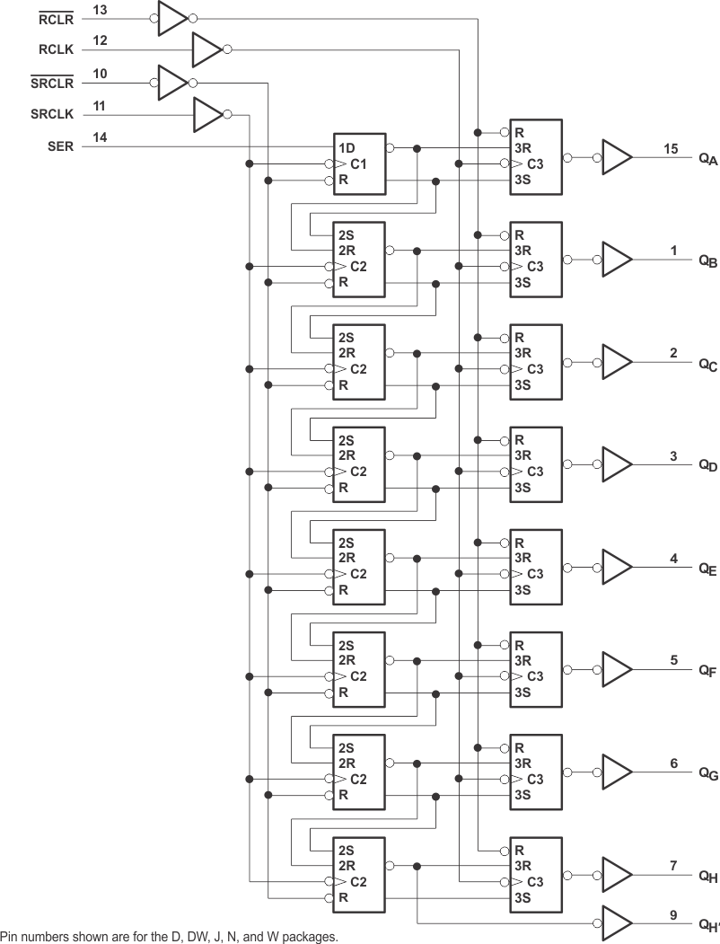
The SNx4HC594 devices contain an 8-bit serial-in, parallel-out shift register that feeds an 8-bit D-type storage register. Separate clocks and direct overriding clear (RCLR, SRCLR) inputs are provided on both the shift and storage registers. A serial (QH’) output is provided for cascading purposes.
Both the shift register (SRCLK) and storage register (RCLK) clocks are positive edge triggered. If both clocks are connected together, the shift register always is one count pulse ahead of the storage register.
The parallel (QA − QH) outputs have high-current capability. QH’ is a standard output.
8.2 Functional Block Diagram
 Figure 5. Logic Diagram (Positive Logic)
8.3 Feature Description
The wide operating range allows the device to be used in a variety of systems that use different logic levels. The high-current outputs allow the device to drive medium loads without significant drops in output voltage. In addition, the low power consumption makes this device a good choice for portable and battery power-sensitive applications.
8.4 Device Functional Modes
Table 1. Function Table
| INPUTS | FUNCTION | ||||
|---|---|---|---|---|---|
| SER | SRCLK | SRCLR | RCLK | RCLR | |
| X | X | L | X | X | Shift register is cleared. |
| L | ↑ | H | X | X | First stage of shift register goes low. Other stages store the data of previous stage, respectively. |
| H | ↑ | H | X | X | First stage of shift register goes high. Other stages store the data of previous stage, respectively. |
| L | ↓ | H | X | X | Shift register state is not changed. |
| X | X | X | X | L | Storage register is cleared. |
| X | X | X | ↑ | H | Shift register data is stored in the storage register. |
| X | X | X | ↓ | H | Storage register state is not changed. |