ZHCSP23B October 2021 – October 2022 SN74HCS541
PRODMIX
- 1 特性
- 2 应用
- 3 说明
- 4 Revision History
- 5 Pin Configuration and Functions
- 6 Specifications
- 7 Parameter Measurement Information
- 8 Detailed Description
- 9 Application and Implementation
- 10Power Supply Recommendations
- 11Layout
- 12Device and Documentation Support
- 13Mechanical, Packaging, and Orderable Information
封装选项
机械数据 (封装 | 引脚)
散热焊盘机械数据 (封装 | 引脚)
- RKS|20
订购信息
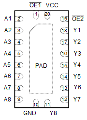
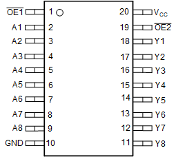
5 Pin Configuration and Functions
 RKS Package,
20-Pin VQFN
(Top View)
 DGS Package,
20-Pin SOT
(Top View)
Table 5-1 Pin Functions
| PIN | TYPE(1) | DESCRIPTION | |
|---|---|---|---|
| NAME | NO. | ||
| OE1 | 1 | I | Output enable input 1, active low |
| A1 | 2 | I | Input for channel 1 |
| A2 | 3 | I | Input for channel 2 |
| A3 | 4 | I | Input for channel 3 |
| A4 | 5 | I | Input for channel 4 |
| A5 | 6 | I | Input for channel 5 |
| A6 | 7 | I | Input for channel 6 |
| A7 | 8 | I | Input for channel 7 |
| A8 | 9 | I | Input for channel 8 |
| GND | 10 | G | Ground |
| Y8 | 11 | O | Output for channel 8 |
| Y7 | 12 | O | Output for channel 7 |
| Y6 | 13 | O | Output for channel 6 |
| Y5 | 14 | O | Output for channel 5 |
| Y4 | 15 | O | Output for channel 4 |
| Y3 | 16 | O | Output for channel 3 |
| Y2 | 17 | O | Output for channel 2 |
| Y1 | 18 | O | Output for channel 1 |
| OE2 | 19 | I | Output enable input 2, active low |
| VCC | 20 | P | Positive supply |
| Thermal Pad(2) | — | The thermal pad can be connect to GND or left floating. Do not connect to any other signal or supply. | |
(1) I = Input, O = Output, I/O = Input or Output, G = Ground, P = Power.
(2) RKS package only.