ZHCSKQ9 January   2020 SN74HCS7002

PRODUCTION DATA.  

  1. 特性
  2. 应用
  3. 说明
    1.     Device Images
      1.      施密特触发输入的优势
  4. 修订历史记录
  5. Pin Configuration and Functions
    1.     Pin Functions
  6. Specifications
    1. 6.1 Absolute Maximum Ratings
    2. 6.2 ESD Ratings
    3. 6.3 Recommended Operating Conditions
    4. 6.4 Thermal Information
    5. 6.5 Electrical Characteristics
    6. 6.6 Switching Characteristics
    7. 6.7 Typical Characteristics
  7. Parameter Measurement Information
  8. Detailed Description
    1. 8.1 Overview
    2. 8.2 Functional Block Diagram
    3. 8.3 Feature Description
      1. 8.3.1 Balanced CMOS Push-Pull Outputs
      2. 8.3.2 CMOS Schmitt-Trigger Inputs
      3. 8.3.3 Clamp Diode Structure
    4. 8.4 Device Functional Modes
  9. Application and Implementation
    1. 9.1 Application Information
    2. 9.2 Typical Application
      1. 9.2.1 Design Requirements
        1. 9.2.1.1 Power Considerations
        2. 9.2.1.2 Input Considerations
        3. 9.2.1.3 Output Considerations
      2. 9.2.2 Detailed Design Procedure
      3. 9.2.3 Application Curves
  10. 10Power Supply Recommendations
  11. 11Layout
    1. 11.1 Layout Guidelines
    2. 11.2 Layout Example
  12. 12器件和文档支持
    1. 12.1 文档支持
      1. 12.1.1 相关文档
    2. 12.2 相关链接
    3. 12.3 社区资源
    4. 12.4 商标
    5. 12.5 静电放电警告
    6. 12.6 Glossary
  13. 13机械、封装和可订购信息

封装选项

机械数据 (封装 | 引脚)
散热焊盘机械数据 (封装 | 引脚)
订购信息

Typical Characteristics

TA = 25°C
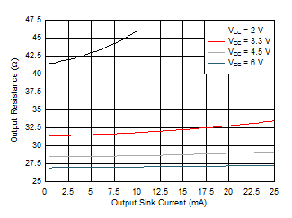
SN74HCS7002 typ_nfet_res.gifFigure 1. Output driver resistance in Low state
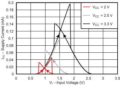
SN74HCS7002 typ-vin-icc-lowv.gifFigure 3. Typical supply current versus input voltage across common supply values (2 V to 3.3 V)
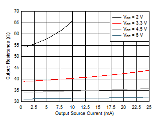
SN74HCS7002 typ_pfet_res.gifFigure 2. Output driver resistance in High state
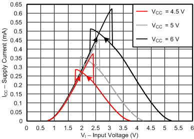
SN74HCS7002 typ-vin-icc-highv.gifFigure 4. Typical supply current versus input voltage across common supply values (4.5 V to 6 V)