SDLS049C December 1983 – November 2016 SN5414 , SN54LS14 , SN7414 , SN74LS14
PRODUCTION DATA.
- 1 Features
- 2 Applications
- 3 Description
- 4 Revision History
- 5 Pin Configuration and Functions
- 6 Specifications
- 7 Parameter Measurement Information
- 8 Detailed Description
- 9 Application and Implementation
- 10Power Supply Recommendations
- 11Layout
- 12Device and Documentation Support
- 13Mechanical, Packaging, and Orderable Information
封装选项
请参考 PDF 数据表获取器件具体的封装图。
机械数据 (封装 | 引脚)
- D|14
- DB|14
- N|14
- NS|14
散热焊盘机械数据 (封装 | 引脚)
订购信息
9 Application and Implementation
NOTE
Information in the following applications sections is not part of the TI component specification, and TI does not warrant its accuracy or completeness. TI’s customers are responsible for determining suitability of components for their purposes. Customers should validate and test their design implementation to confirm system functionality.
9.1 Application Information
The SNx414 and SNx4LS14 device is a Schmitt-Trigger input CMOS device that can be used for a multitude of inverting buffer type functions. The application shown here takes advantage of the Schmitt-Trigger inputs to produce a delay for a logic input.
9.2 Typical Application
 Figure 28. Simplified Application Schematic
9.2.1 Design Requirements
This device uses CMOS technology. Take care to avoid bus contention because it can drive currents that would exceed maximum limits. Parallel output drive can create fast edges into light loads, so consider routing and load conditions to prevent ringing.
9.2.2 Detailed Design Procedure
This circuit is designed around an RC network that produces a slow input to the second inverter. The RC time constant (τ) is calculated from: τ = RC.
The delay time for this circuit is from tdelay(min) = –ln |1 – VT+(min) / VCC| τ to tdelay(max) = –ln |1 – VT+(max) / VCC| τ. It must be noted that the delay is consistent for each device, but because the switching threshold is only ensured between the minimum and maximum value, the output pulse length varies between devices. These values must be calculated by using the minimum and maximum ensured VT+ values in the Electrical Characteristics.
The resistor value must be chosen such that the maximum current to and from the SNx414/SNx4LS14 is 8 mA at
5-V VCC.
9.2.3 Application Curve
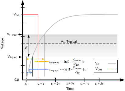 Figure 29. Ideal Capacitor Voltage and Output Voltage With Positive Switching Threshold
9.3 System Examples
Here are some examples of various applications using the SNx414 and SNx4LS14 device.
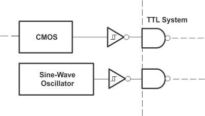 Figure 30. TTL System Interface For Slow Input Waveforms
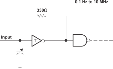 Figure 32. Multivibrator
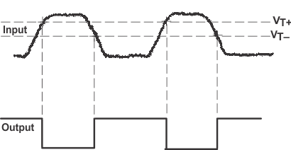 Figure 31. Pulse Shaper
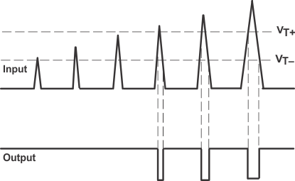 Figure 33. Threshold Detector
 Figure 34. Pulse Stretcher