SDLS153A January 1981 – January 2016 SN74LS292 , SN74LS294
PRODUCTION DATA.
- 1 Features
- 2 Applications
- 3 Description
- 4 Revision History
- 5 Pin Configuration and Functions
- 6 Specifications
- 7 Parameter Measurement Information
- 8 Detailed Description
- 9 Application and Implementation
- 10Power Supply Recommendations
- 11Layout
- 12Device and Documentation Support
- 13Mechanical, Packaging, and Orderable Information
9 Application and Implementation
NOTE
Information in the following applications sections is not part of the TI component specification, and TI does not warrant its accuracy or completeness. TI’s customers are responsible for determining suitability of components for their purposes. Customers should validate and test their design implementation to confirm system functionality.
9.1 Application Information
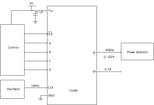
This device is used for configurable frequency, programmable frequency, and timing division as shown in Typical Application.
9.2 Typical Application
 Figure 10. Typical application
9.2.1 Design Requirements
This device does not have balanced output drive. Take care to avoid bus contention because it can sink currents that would exceed maximum limits. The high drive will also create fast edges into light loads so routing and load conditions should be considered to prevent ringing.
9.2.2 Detailed Design Procedure
- Recommended Input Conditions:
- Rise time and fall time specs. See (Δt/ΔV) in Recommended Operating Conditions.
- Specified high and low levels. See (VIH and VIL) in Recommended Operating Conditions.
- Inputs can go as high as (VI max) in Recommended Operating Conditions at any valid VCC.
- Recommended Output Conditions:
- Load currents should not exceed (IOH,IOL) per output. These limits are located in the Recommended Operating Conditions.
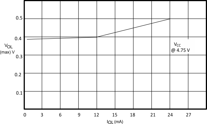
9.2.3 Application Curve
 Figure 11. VOL vs IOL