SDLS153A January 1981 – January 2016 SN74LS292 , SN74LS294
PRODUCTION DATA.
- 1 Features
- 2 Applications
- 3 Description
- 4 Revision History
- 5 Pin Configuration and Functions
- 6 Specifications
- 7 Parameter Measurement Information
- 8 Detailed Description
- 9 Application and Implementation
- 10Power Supply Recommendations
- 11Layout
- 12Device and Documentation Support
- 13Mechanical, Packaging, and Orderable Information
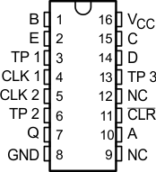
5 Pin Configuration and Functions
SN74LS29x J, W, or N Package
16-Pin PDIP
Top View

Pin Functions, SN74LS292
| PIN | I/O | DESCRIPTION | |
|---|---|---|---|
| NAME | PDIP | ||
| A | 10 | I | Programming input A |
| B | 1 | I | Programming input B |
| C | 15 | I | Programming input C |
| CLK1 | 4 | I | Clock 1 input |
| CLK2 | 5 | I | Clock 2 input |
| CLR | 11 | I | Active-low clear input |
| D | 14 | I | Programming input D |
| E | 2 | I | Programming input E |
| GND | 8 | - | Ground |
| NC | 9, 12 | - | No connect |
| Q | 7 | O | Q Output |
| TP | — | O | Test Point |
| TP1 | 3 | O | Test Point |
| TP2 | 6 | O | Test Point |
| TP3 | 13 | O | Test Point |
| VCC | 16 | - | Power |
Pin Functions, SN74LS294
| PIN | I/O | DESCRIPTION | |
|---|---|---|---|
| NAME | PDIP | ||
| A | 2 | I | Programming input A |
| B | 1 | I | Programming input B |
| C | 15 | I | Programming input C |
| CLK1 | 4 | I | Clock 1 input |
| CLK2 | 5 | I | Clock 2 input |
| CLR | 11 | I | Active-low clear input |
| D | 14 | I | Programming input D |
| E | — | I | Programming input E |
| GND | 8 | - | Ground |
| NC | 6, 9 ,10, 12, 13 | - | No connect |
| Q | 7 | O | Q Output |
| TP | 3 | O | Test Point |
| TP1 | — | O | Test Point |
| TP2 | — | O | Test Point |
| TP3 | — | O | Test Point |
| VCC | 16 | - | Power |