SCLS467F FEBRUARY 2003 – June 2016 SN74LV123A-Q1
PRODUCTION DATA.
- 1 Features
- 2 Applications
- 3 Description
- 4 Revision History
- 5 Pin Configuration and Functions
-
6 Specifications
- 6.1 Absolute Maximum Ratings
- 6.2 ESD Ratings
- 6.3 Recommended Operating Conditions
- 6.4 Thermal Information
- 6.5 Electrical Characteristics
- 6.6 Timing Requirements — VCC = 3.3 V ± 0.3 V
- 6.7 Timing Requirements — VCC = 5 V ± 0.5 V
- 6.8 Switching Characteristics — VCC = 3.3 V ± 0.3 V
- 6.9 Switching Characteristics — VCC = 5 V ± 0.5 V
- 6.10 Operating Characteristics
- 6.11 Typical Characteristics
- 7 Parameter Measurement Information
- 8 Detailed Description
- 9 Application and Implementation
- 10Power Supply Recommendations
- 11Layout
- 12Device and Documentation Support
- 13Mechanical, Packaging, and Orderable Information
8 Detailed Description
8.1 Overview
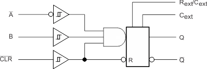
This edge-triggered multivibrator features output pulse-duration control by three methods. In the first method, the A input is low, and the B input goes high. In the second method, the B input is high, and the A input goes low. In the third method, the A input is low, the B input is high, and the clear (CLR) input goes high.
The output pulse duration is programmable by selecting external resistance and capacitance values. The external timing capacitor must be connected between Cext and Rext/Cext (positive) and an external resistor connected between Rext/Cext and VCC. Connect an external variable resistance between Rext/Cext and VCCto obtain variable pulse durations. The output pulse duration also can be reduced by taking CLR low.
Pulse triggering occurs at a particular voltage level and is not directly related to the transition time of the input pulse. The A, B, and CLR inputs have Schmitt triggers with sufficient hysteresis to handle slow input transition rates with jitter-free triggering at the outputs.
When triggered, the basic pulse duration can be extended by retriggering the gated low-level-active (A) or high-level-active (B) input. Pulse duration may be reduced by taking CLR low. The input-output timing diagram (Figure 1) shows pulse control by retriggering the inputs and early clearing.
The Q outputs are in the low state, and the Q outputs are in the high state during power up. The outputs are glitch free, without applying a reset pulse.
This device is fully specified for partial-power-down applications using Ioff. The Ioff circuitry disables the outputs, which prevents damaging current backflow through the device when it is powered down.
8.2 Functional Block Diagram
 Figure 10. Logic Diagram, Each Multivibrator (Positive Logic)
8.3 Feature Description
The SN74LV123A operates over a wide supply range from 2 V to 5.5 V. The propagation delay has a maximum of 11 ns at 5-V supply. The typical output ground bounce is less than 0.8 V at 3.3-V supply and 25°C. The typical output VOH undershoot is greater than 2.3 V at 3.3-V supply and 25°C.
These parts support mixed-mode voltage operation on all ports.
Schmitt-trigger circuitry on the A, B, and CLR inputs allow for slow input transition rates and noisy input signals.
This device can be configured for rising or falling edge triggering.
This device supports partial-power-down mode operation.
This device is retriggerable for very long output pulses up to 100% duty cycle.
The clear signal overrides an output pulse and terminates it early.
Glitch-free power-up reset on outputs.
8.3.1 Power-Down Considerations
Large values of Cext can cause problems when powering down the SN74LV123A-Q1 devices because of the amount of energy stored in the capacitor. When a system containing this device is powered down, the capacitor can discharge from VCC through the protection diodes at pin 2 or pin 14. Current through the input protection diodes must be limited to 30 mA; therefore, the turn-off time of the VCC power supply must not be faster than t = VCC × Cext / 30 mA. For example, if VCC = 5 V and Cext = 15 pF, the VCC supply must turn off no faster than t = (5 V) × (15 pF) / 30 mA = 2.5 ns. Usually, this is not a problem because power supplies are heavily filtered and cannot discharge at this rate. The SN74LV123A-Q1 devices can sustain damage when a more rapid decrease of VCC to zero occurs. Use external clamping diodes to avoid this possibility.
8.4 Device Functional Modes
Table 1 shows the functional modes for each monostable multivibrator in the SN74LV123A-Q1.
Table 1. Function Table
(Each Multivibrator)
| INPUTS | OUTPUTS | |||
|---|---|---|---|---|
| CLR | A | B | Q | Q |
| L | X | X | L | H |
| X | H | X | L(1) | H(1) |
| X | X | L | L(1) | H(1) |
| H | L | ↑ |  |
 |
| H | ↓ | H |  |
 |
| ↑ | L | H |  |
 |