SCLS393Q APRIL 1998 – August 2015 SN74LV123A
UNLESS OTHERWISE NOTED, this document contains PRODUCTION DATA.
- 1 Features
- 2 Applications
- 3 Description
- 4 Revision History
- 5 Description (continued)
- 6 Pin Configuration and Functions
-
7 Specifications
- 7.1 Absolute Maximum Ratings
- 7.2 ESD Ratings
- 7.3 Recommended Operating Conditions
- 7.4 Thermal Information
- 7.5 Electrical Characteristics
- 7.6 Timing Requirements, VCC = 2.5 V ± 0.2 V
- 7.7 Timing Requirements, VCC = 3.3 V ± 0.3 V
- 7.8 Timing Requirements, VCC = 5 V ± 0.5 V
- 7.9 Switching Characteristics, VCC = 2.5 V ± 0.2 V
- 7.10 Switching Characteristics, VCC = 3.3 V ± 0.3 V
- 7.11 Switching Characteristics, VCC = 5 V ± 0.5 V
- 7.12 Operating Characteristics
- 7.13 Typical Characteristics
- 8 Parameter Measurement Information
- 9 Detailed Description
- 10Application and Implementation
- 11Power Supply Recommendations
- 12Layout
- 13Device and Documentation Support
- 14Mechanical, Packaging, and Orderable Information
封装选项
机械数据 (封装 | 引脚)
散热焊盘机械数据 (封装 | 引脚)
- RGY|16
订购信息
6 Pin Configuration and Functions
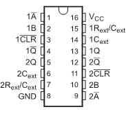
D, DB, DGV, NS, or PW Package
16-Pin SOIC, SSOP, SO, TSSOP
Top View

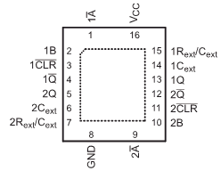
RGY Package
16-Pin VQFN
Top View

Pin Functions
| PIN | I/O | DESCRIPTION | |
|---|---|---|---|
| NAME | NO. | ||
| 1A | 1 | I | Channel 1 falling edge trigger input when 1B = L; Hold low for other input methods |
| 1B | 2 | I | Channel 1 rising edge trigger input when 1A = H; Hold high for other input methods |
| 1CLR | 3 | I | Channel 1 rising edge trigger when 1A = H and 1B = L; Hold high for other input methods; Can cut pulse length short by driving low during output |
| 1Q | 4 | O | Channel 1 inverted output |
| 2Q | 5 | O | Channel 2 output |
| 2Cext | 6 | — | Channel 2 external capacitor negative connection |
| 2Rext/Cext | 7 | — | Channel 2 external capacitor and resistor junction connection |
| GND | 8 | — | Ground |
| 2A | 9 | I | Channel 2 falling edge trigger input when 2B = L; Hold low for other input methods |
| 2B | 10 | I | Channel 2 rising edge trigger input when 2A = H; Hold high for other input methods |
| 2CLR | 11 | I | Channel 2 rising edge trigger when 2A = H and 2B = L; Hold high for other input methods; Can cut pulse length short by driving low during output |
| 2Q | 12 | O | Channel 2 inverted output |
| 1Q | 13 | O | Channel 1 output |
| 1Cext | 14 | — | Channel 1 external capacitor negative connection |
| 1Rext/Cext | 15 | — | Channel 1 external capacitor and resistor junction connection |
| VCC | 16 | — | Power supply |