ZHCSRG4N April 1998 – March 2023 SN74LV138A
PRODMIX
- 1 特性
- 2 应用
- 3 说明
- 4 Revision History
- 5 Pin Configuration and Functions
-
6 Specifications
- 6.1 Absolute Maximum Ratings
- 6.2 ESD Ratings
- 6.3 Recommended Operating Conditions #GUID-332E8763-FFB4-457A-A681-FBA0609A5CEC/NSCES129_8420041244441
- 6.4 Thermal Information
- 6.5 Electrical Characteristics
- 6.6 Switching Characteristics, VCC = 2.5 V ± 0.25 V
- 6.7 Switching Characteristics, VCC = 3.3 V ± 0.3 V
- 6.8 Switching Characteristics, VCC = 5 V ± 0.5 V
- 6.9 Operating Characteristics
- 6.10 Typical Characteristics
- 7 Parameter Measurement Information
- 8 Detailed Description
- 9 应用和实施
- 10Device and Documentation Support
- 11Mechanical, Packaging, and Orderable Information
封装选项
请参考 PDF 数据表获取器件具体的封装图。
机械数据 (封装 | 引脚)
- DB|16
- PW|16
- BQB|16
- NS|16
- RGY|16
- D|16
- DGV|16
散热焊盘机械数据 (封装 | 引脚)
订购信息
5 Pin Configuration and Functions
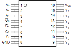
 Figure 5-1 D, DB, DGV, NS and PW Package 16-Pin (Top View)
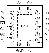
 Figure 5-2 RGY and BQB Package 16-Pin (Top View)
Table 5-1 Pin Functions
| PIN | TYPE(1) | DESCRIPTION | |
|---|---|---|---|
| NAME | NO. | ||
| A0 | 1 | I | Address select 0 |
A1 | 2 | I | Address select 1 |
A2 | 3 | I | Address select 2 |
| G2 | 6 | I | Strobe input |
| G0 | 4 | I | Strobe input, active low |
| G1 | 5 | I | Strobe input, active low |
| GND | 8 | G | Ground |
| VCC | 16 | P | Positive supply |
| Y0 | 15 | O | Output 0 |
| Y1 | 14 | O | Output 1 |
| Y2 | 13 | O | Output 2 |
| Y3 | 12 | O | Output 3 |
| Y4 | 11 | O | Output 4 |
| Y5 | 10 | O | Output 5 |
| Y6 | 9 | O | Output 6 |
Y7 | 7 | O | Output 7 |
| Thermal Pad | - | Thermal Pad(2) | |
(1) Signal Types: I = Input, O = Output, I/O = Input or Output, G = Ground, P = Power
(2) BQB and RGY package only