ZHCSRJ1A january   2023  – august 2023 SN74LV165B-EP

PRODUCTION DATA  

  1.   1
  2. 特性
  3. 应用
  4. 说明
  5. Revision History
  6. Pin Configuration and Functions
  7. Specifications
    1. 6.1  Absolute Maximum Ratings
    2. 6.2  ESD Ratings
    3. 6.3  Recommended Operating Conditions
    4. 6.4  Thermal Information
    5. 6.5  Electrical Characteristics
    6. 6.6  Timing Requirements, VCC = 2.5 V ± 0.2 V
    7. 6.7  Timing Requirements, VCC = 3.3 V ± 0.3 V
    8. 6.8  Timing Requirements, VCC = 5 V ± 0.5 V
    9. 6.9  Switching Characteristics, VCC = 2.5 V ± 0.2 V
    10. 6.10 Switching Characteristics, VCC = 3.3 V ± 0.3 V
    11. 6.11 Switching Characteristics, VCC = 5 V ± 0.5 V
    12. 6.12 Operating Characteristics
    13. 6.13 Typical Characteristics
  8. Parameter Measurement Information
  9. Detailed Description
    1. 8.1 Overview
    2. 8.2 Functional Block Diagram
    3. 8.3 Feature Description
      1. 8.3.1 Balanced CMOS Push-Pull Outputs
      2. 8.3.2 Latching Logic
      3. 8.3.3 Partial Power Down (Ioff)
      4. 8.3.4 Clamp Diode Structure
    4. 8.4 Device Functional Modes
  10. Application and Implementation
    1. 9.1 Application Information
    2. 9.2 Typical Application
      1. 9.2.1 Power Considerations
      2. 9.2.2 Input Considerations
      3. 9.2.3 Output Considerations
      4. 9.2.4 Detailed Design Procedure
      5. 9.2.5 Application Curves
    3. 9.3 Power Supply Recommendations
    4. 9.4 Layout
      1. 9.4.1 Layout Guidelines
      2. 9.4.2 Layout Example
  11. 10Device and Documentation Support
    1. 10.1 Related Documentation
    2. 10.2 Receiving Notification of Documentation Updates
    3. 10.3 支持资源
    4. 10.4 Trademarks
    5. 10.5 静电放电警告
    6. 10.6 术语表
  12. 11Mechanical, Packaging, and Orderable Information

封装选项

请参考 PDF 数据表获取器件具体的封装图。

机械数据 (封装 | 引脚)
  • PW|16
散热焊盘机械数据 (封装 | 引脚)
订购信息

Typical Characteristics

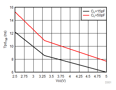
GUID-E51B68BB-898B-4528-AA9F-2A7D670CEE7D-low.gifFigure 6-2 TPD Typical (25°C) vs Vcc