ZHCSBY3D December   2013  – February 2024 SN74LV1T126

PRODUCTION DATA  

  1.   1
  2. 特性
  3. 应用
  4. 说明
  5. Related Products
  6. Pin Configuration and Functions
  7. Specifications
    1. 6.1 Absolute Maximum Ratings
    2. 6.2 ESD Ratings
    3. 6.3 Recommended Operating Conditions
    4. 6.4 Thermal Information
    5. 6.5 Electrical Characteristics
    6. 6.6 Switching Characteristics
    7. 6.7 Operating Characteristics
    8. 6.8 Typical Characteristics
  8. Parameter Measurement Information
  9. Detailed Description
    1. 8.1 Overview
    2. 8.2 Functional Block Diagram
    3. 8.3 Feature Description
      1. 8.3.1 Clamp Diode Structure
      2. 8.3.2 Balanced CMOS Push-Pull Outputs
      3. 8.3.3 LVxT Enhanced Input Voltage
        1. 8.3.3.1 Down Translation
        2. 8.3.3.2 Up Translation
    4. 8.4 Device Functional Modes
  10. 应用信息免责声明
    1. 9.1 Power Supply Recommendations
    2. 9.2 Layout
      1. 9.2.1 Layout Guidelines
  11. 10Device and Documentation Support
    1. 10.1 Documentation Support (Analog)
      1. 10.1.1 Related Documentation
    2. 10.2 接收文档更新通知
    3. 10.3 支持资源
    4. 10.4 Trademarks
    5. 10.5 静电放电警告
    6. 10.6 术语表
  12. 11Revision History
  13. 12Mechanical, Packaging, and Orderable Information

封装选项

机械数据 (封装 | 引脚)
散热焊盘机械数据 (封装 | 引脚)
订购信息

Typical Characteristics

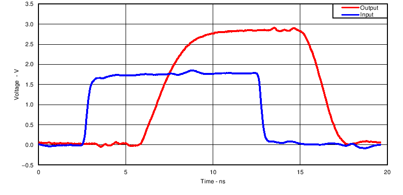
GUID-FB6E5726-DA2D-4A1C-80B0-71DC53C12B56-low.png
Figure 6-1 Switching Characteristics at 50 MHz
Excellent Signal Integrity
(1.8 V to 3.3 V at 3.3-V VCC)
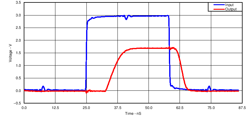
GUID-B61EC6FF-97CA-4A63-89BF-E6C66661CA42-low.png
Figure 6-3 Switching Characteristics at 15 MHz
Excellent Signal Integrity
(3.3 V to 1.8 V at 1.8-V VCC)
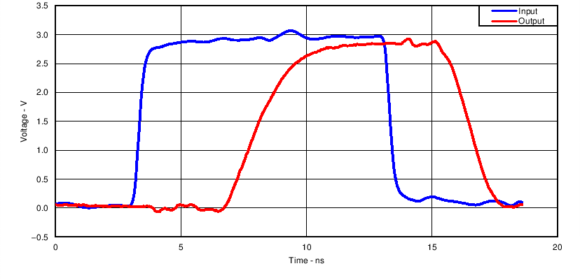
GUID-72016395-52C6-4156-9778-71D4F8991006-low.png
Figure 6-2 Switching Characteristics at 50 MHz
Excellent Signal Integrity
(3.3 V to 3.3 V at 3.3-V VCC)