ZHCSBY2E December   2013  – February 2024 SN74LV1T34

PRODUCTION DATA  

  1.   1
  2. 特性
  3. 应用
  4. 说明
  5. Related Products
  6. Pin Configuration and Functions
  7. Specifications
    1. 6.1 Absolute Maximum Ratings
    2. 6.2 ESD Ratings
    3. 6.3 Recommended Operating Conditions
    4. 6.4 Thermal Information
    5. 6.5 Electrical Characteristics
    6. 6.6 Switching Characteristics
    7. 6.7 Operating Characteristics
    8. 6.8 Typical Characteristics
  8. Parameter Measurement Information
  9. Detailed Description
    1. 8.1 Overview
    2. 8.2 Functional Block Diagram
    3. 8.3 Feature Description
      1. 8.3.1 Clamp Diode Structure
      2. 8.3.2 Balanced CMOS Push-Pull Outputs
      3. 8.3.3 LVxT Enhanced Input Voltage
        1. 8.3.3.1 Down Translation
        2. 8.3.3.2 Up Translation
    4. 8.4 Device Functional Modes
  10. Application and Implementation
    1. 9.1 Power Supply Recommendations
    2. 9.2 Layout
      1. 9.2.1 Layout Guidelines
  11. 10Device and Documentation Support
    1. 10.1 Documentation Support (Analog)
      1. 10.1.1 Related Documentation
    2. 10.2 接收文档更新通知
    3. 10.3 支持资源
    4. 10.4 Trademarks
    5. 10.5 静电放电警告
    6. 10.6 术语表
  12. 11Revision History
  13. 12Mechanical, Packaging, and Orderable Information

封装选项

机械数据 (封装 | 引脚)
散热焊盘机械数据 (封装 | 引脚)
订购信息

Clamp Diode Structure

The outputs to this device have both positive and negative clamping diodes, and the inputs to this device have negative clamping diodes only as depicted in Figure 8-2.

CAUTION: Voltages beyond the values specified in the Absolute Maximum Ratings table can cause damage to the device. The input and output voltage ratings may be exceeded if the input and output clamp-current ratings are observed.
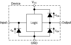
GUID-90BA7574-3857-40F6-BEE6-72C3739CC258-low.gifFigure 8-2 Electrical Placement of Clamping Diodes for Each Input and Output