ZHCSWI9H August 2003 – October 2024 SN74LV4051A-Q1
PRODUCTION DATA
- 1
- 1 特性
- 2 应用
- 3 说明
- 4 Pin Configuration and Functions
-
5 Specifications
- 5.1 Absolute Maximum Ratings
- 5.2 ESD Ratings
- 5.3 Thermal Information: SN74LV4051A-Q1
- 5.4 Recommended Operating Conditions
- 5.5 Electrical Characteristics
- 5.6 Timing Characteristics VCC = 2.5 V ± 0.2 V
- 5.7 Timing Characteristics VCC = 3.3 V ± 0.3 V
- 5.8 Timing Characteristics VCC = 5 V ± 0.5 V
- 5.9 AC Characteristics
- 6 Parameter Measurement Information
- 7 Detailed Description
- 8 Application and Implementation
- 9 Device and Documentation Support
- 10Revision History
- 11Mechanical, Packaging, and Orderable Information
封装选项
请参考 PDF 数据表获取器件具体的封装图。
机械数据 (封装 | 引脚)
- PW|16
- DYY|16
- DW|16
- D|16
散热焊盘机械数据 (封装 | 引脚)
- DW|16
订购信息
6 Parameter Measurement Information
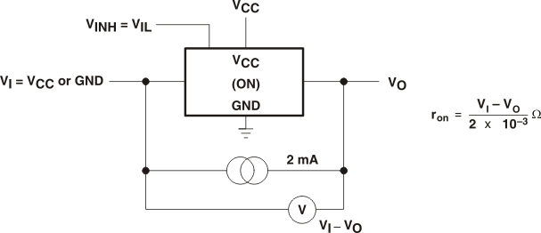 Figure 6-1 On-State
Resistance Test Circuit
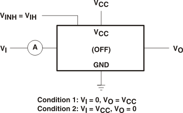 Figure 6-2 Off-State
Switch Leakage-Current Test Circuit
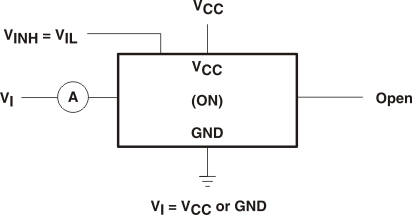 Figure 6-3 On-State
Switch Leakage-Current Test Circuit
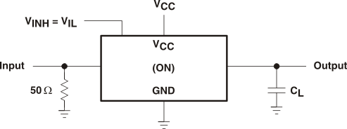 Figure 6-4 Propagation Delay Time, Signal Input to Signal Output
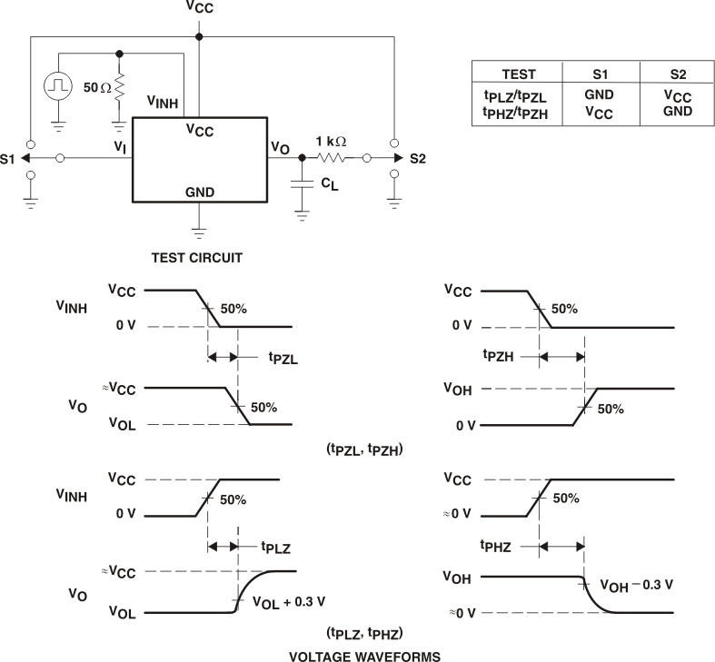 Figure 6-5 Switching
Time (tPZL, tPLZ, tPZH, tPHZ),
Control to Signal Output
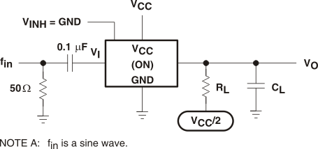 Figure 6-6 Frequency
Response (Switch On)
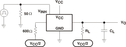 Figure 6-7 Crosstalk
(Control Input, Switch Output)
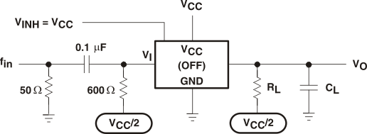 Figure 6-8 Feedthrough Attenuation (Switch Off)
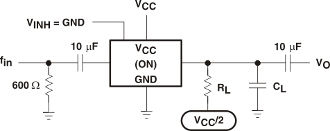 Figure 6-9 Sine-Wave
Distortion