SCLS381M August 1997 – March 2015 SN74LV74A
UNLESS OTHERWISE NOTED, this document contains PRODUCTION DATA.
- 1 Features
- 2 Applications
- 3 Description
- 4 Revision History
- 5 Pin Configuration and Functions
-
6 Specifications
- 6.1 Absolute Maximum Ratings
- 6.2 ESD Ratings
- 6.3 Recommended Operating Conditions
- 6.4 Electrical Characteristics
- 6.5 Switching Characteristics: VCC = 2.5 V ± 0.2 V
- 6.6 Switching Characteristics: VCC = 3.3 V ± 0.3 V
- 6.7 Switching Characteristics: VCC = 5 V ± 0.5 V
- 6.8 Timing Requirements: VCC = 2.5 V ± 0.2 V
- 6.9 Timing Requirements: VCC = 3.3 V ± 0.3 V
- 6.10 Timing Requirements: VCC = 5 V ± 0.5 V
- 6.11 Noise Characteristics
- 6.12 Operating Characteristics
- 6.13 Typical Characteristics
- 7 Parameter Measurement Information
- 8 Detailed Description
- 9 Application and Implementation
- 10Power Supply Recommendations
- 11Layout
- 12Device and Documentation Support
- 13Mechanical, Packaging, and Orderable Information
封装选项
请参考 PDF 数据表获取器件具体的封装图。
机械数据 (封装 | 引脚)
- D|14
- RGY|14
- DGV|14
- PW|14
- DB|14
- NS|14
散热焊盘机械数据 (封装 | 引脚)
订购信息
5 Pin Configuration and Functions
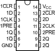
D, DGV, NS, or PW Package
14-PIN SOIC, SOP, SSOP, or TSSOP
Top View

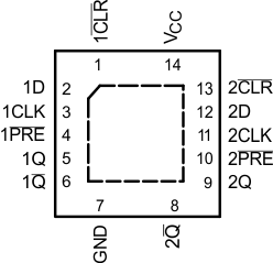
RGY Package
14-PIN VQFN
Top View

Pin Functions
| PIN | I/O | DESCRIPTION | |
|---|---|---|---|
| NO. | NAME | ||
| 1 | 1CLR | I | 1 clear |
| 2 | 1D | I | 1D input |
| 3 | 1CLK | I | 1 clock |
| 4 | 1PRE | I | 1 preset |
| 5 | 1Q | O | 1Q output |
| 6 | 1Q | O | 1Q output |
| 7 | GND | – | GND |
| 8 | 2Q | O | 2Q output |
| 9 | 2Q | O | 2Q output |
| 10 | 2PRE | I | 2 preset |
| 11 | 2CLK | I | 2 clock |
| 12 | 2D | I | 2D input |
| 13 | 2CLR | I | 2 clear |
| 14 | Vcc | – | Supply voltage input |