ZHCSK17AC March 1993 – April 2022 SN54LVC14A , SN74LVC14A
PRODUCTION DATA
- 1 特性
- 2 应用
- 3 说明
- 4 Revision History
- 5 Pin Configuration and Functions
-
6 Specifications
- 6.1 Absolute Maximum Ratings
- 6.2 ESD Ratings
- 6.3 Recommended Operating Conditions: SN54LVC14A
- 6.4 Recommended Operating Conditions: SN74LVC14A
- 6.5 Thermal Information
- 6.6 Electrical Characteristics, SN54LVC14A
- 6.7 Electrical Characteristics, SN74LVC14A
- 6.8 Switching Characteristics, SN54LVC14A
- 6.9 Switching Characteristics, SN74LVC14A
- 6.10 Operating Characteristics
- 6.11 Typical Characteristics
- 7 Parameter Measurement Information
- 8 Detailed Description
- 9 Application and Implementation
- 10Power Supply Recommendations
- 11Layout
- 12Device and Documentation Support
- 13Mechanical, Packaging, and Orderable Information
封装选项
请参考 PDF 数据表获取器件具体的封装图。
机械数据 (封装 | 引脚)
- D|14
- RGY|14
- DB|14
- PW|14
- DGV|14
- NS|14
散热焊盘机械数据 (封装 | 引脚)
- RGY|14
订购信息
8.3.3 Clamp Diodes
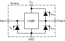
The inputs to this device have negative clamping diodes. The outputs to this device have both positive and negative clamping diodes as shown in Figure 8-2.
CAUTION: Voltages beyond the values
specified in the Absolute Maximum Ratings table can cause damage to the device.
The input negative-voltage and output voltage ratings may be exceeded if the input
and output clamp-current ratings are observed.
 Figure 8-2 Electrical Placement of Clamping Diodes for Each Input and Output