SCES636B AUGUST 2005 – April 2015 SN74LVC16T245
PRODUCTION DATA.
- 1 Features
- 2 Applications
- 3 Description
- 4 Revision History
- 5 Description (continued)
- 6 Pin Configuration and Functions
-
7 Specifications
- 7.1 Absolute Maximum Ratings
- 7.2 ESD Ratings
- 7.3 Recommended Operating Conditions
- 7.4 Thermal Information
- 7.5 Electrical Characteristics
- 7.6 Switching Characteristics: VCCA = 1.8 V ±0.15 V
- 7.7 Switching Characteristics: VCCA = 2.5 V ±0.2 V
- 7.8 Switching Characteristics: VCCA = 3.3 V ±0.3 V
- 7.9 Switching Characteristics: VCCA = 5 V ±0.5 V
- 7.10 Operating Characteristics
- 7.11 Typical Characteristics
- 8 Parameter Measurement Information
- 9 Detailed Description
- 10Application and Implementation
- 11Power Supply Recommendations
- 12Layout
- 13Device and Documentation Support
- 14Mechanical, Packaging, and Orderable Information
封装选项
请参考 PDF 数据表获取器件具体的封装图。
机械数据 (封装 | 引脚)
- DGG|48
- DL|48
- DGV|48
散热焊盘机械数据 (封装 | 引脚)
订购信息
9 Detailed Description
9.1 Overview
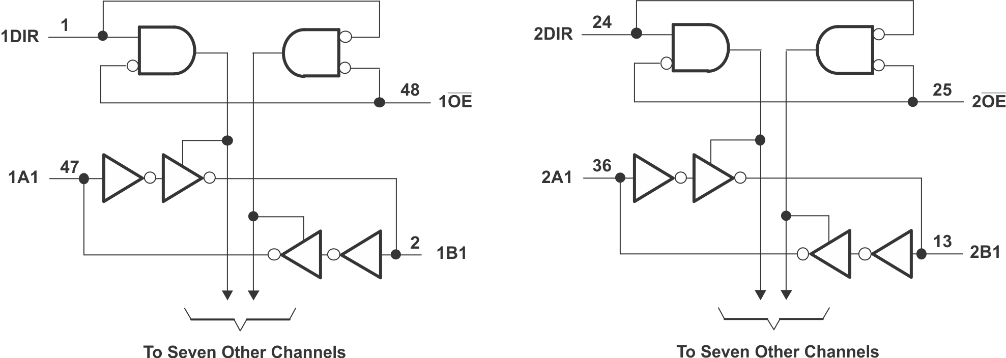
The SN74LVC16T245 is a 16-bit, dual-supply noninverting bidirectional voltage level translation. Pins A and control pins (DIR and OE) are supported by VCCA and pins B are supported by VCCB. The A port is able to accept I/O voltages ranging from 1.65 V to 5.5 V, while the B port can accept I/O voltages from 1.65 V to 5.5 V. A high on DIR allows data transmission from A to B and a low on DIR allows data transmission from B to A when OE is set to low. When OE is set to high, both A and B are in the high-impedance state.
This device is fully specified for partial-power-down applications using off output current (Ioff).
The VCC isolation feature ensures that if either VCC input is at GND, both ports are put in a high-impedance state.
9.2 Functional Block Diagram

9.3 Feature Description
9.3.1 Fully Configurable Dual-Rail Design Allows Each Port to Operate Over the Full 1.65-V to 5.5-V Power-Supply Range
Both VCCA and VCCB can be supplied at any voltage from 1.65 V to 5.5 V making the device suitable for translating between any of the low voltage nodes (1.8-V, 2.5-V, and 3.3-V).
9.3.2 Support High-Speed Translation
SN74LVC16T245 can support high data rate application. Data rates can be calculated form the maximum propagation delay. This is also dependant on the output load. For example, for a 3.3-V to 5-V conversion, the maximum frequency is 200 MHz.
9.3.3 Partial-Power-Down Mode Operation
This device is fully specified for partial-power-down applications using off output current (Ioff). Ioff will prevent backflow current by disabling I/O output circuits when device is in partial power-down mode.
9.3.4 VCC Isolation
The VCC isolation feature ensures that if either VCCA or VCCB are at GND, both ports will be in a high-impedance state (IOZ shown in Electrical Characteristics). This prevents false logic levels from being presented to either bus.
9.4 Device Functional Modes
The functional modes for the SN74LVC16T245 device are shown in Table 1.
Table 1. Function Table(1)
(Each Transceiver)
| CONTROL INPUTS | OUTPUT CIRCUITS | OPERATION | ||
|---|---|---|---|---|
| OE | DIR | A PORT | B PORT | |
| L | L | Enabled | Hi-Z | B data to A bus |
| L | H | Hi-Z | Enabled | A data to B bus |
| H | X | Hi-Z | Hi-Z | Isolation |