SCES218Y APRIL 1999 – November 2018 SN74LVC1G14
PRODUCTION DATA.
- 1 Features
- 2 Applications
- 3 Description
- 4 Revision History
- 5 Pin Configuration and Functions
- 6 Specifications
- 7 Parameter Measurement Information
- 8 Detailed Description
- 9 Application and Implementation
- 10Power Supply Recommendations
- 11Layout
- 12Device and Documentation Support
- 13Mechanical, Packaging, and Orderable Information
封装选项
请参考 PDF 数据表获取器件具体的封装图。
机械数据 (封装 | 引脚)
- DPW|5
- DBV|5
- DSF|6
- DCK|5
- YZV|4
- DRL|5
- YZP|5
- DRY|6
散热焊盘机械数据 (封装 | 引脚)
订购信息
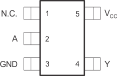
5 Pin Configuration and Functions
DCK Package
5-Pin SC70
Top View
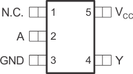
DRL Package
5-Pin SOT-5X3
Top View

DRY Package
6-Pin SON
Top View

DPW Package
5-Pin X2SON
Top View

DSF Package
6-Pin SON
Top View
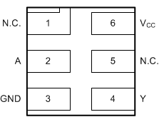
See mechanical drawings for dimensions.
N.C. – No internal connection
YZP Package
5-Pin DSBGA
Bottom View
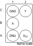
DNU – Do not use
YZV Package
4-Pin DSBGA
Bottom View
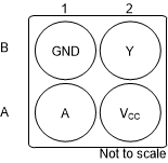
Pin Functions
| PIN | I/O | DESCRIPTION | ||||
|---|---|---|---|---|---|---|
| NAME | DBV, DCK, DRL, DPW | DRY, DSF | YZP | YZV | ||
| A | 2 | 2 | B1 | A1 | I | Signal Input |
| GND | 3 | 3 | C1 | B1 | — | Ground |
| N.C. | 1 | 1, 5 | — | — | — | No internal connection(1) |
| DNU | — | — | A1 | — | — | Do not use(2) |
| VCC | 5 | 6 | A2 | A2 | — | Positive Supply |
| Y | 4 | 4 | C2 | B2 | O | Signal Output |
(1) Pins labeled N.C. can be connected to any signal or voltage source, including ground. They should always be soldered to the board.
(2) Pins labeled DNU should not be connected to any signal or voltage source, including ground. They should always be soldered to the board.
