SCES218Y APRIL   1999  – November 2018 SN74LVC1G14

PRODUCTION DATA.  

  1. Features
  2. Applications
  3. Description
    1.     Device Images
      1.      Logic Diagram (Positive Logic) (DBV, DCK, DRL, DRY, DPW, and YZP Package)
      2.      Logic Diagram (Positive Logic) (YZV Package)
  4. Revision History
  5. Pin Configuration and Functions
    1.     Pin Functions
  6. Specifications
    1. 6.1 Absolute Maximum Ratings
    2. 6.2 ESD Ratings
    3. 6.3 Recommended Operating Conditions
    4. 6.4 Thermal Information
    5. 6.5 Electrical Characteristics
    6. 6.6 Switching Characteristics: –40°C to 85°C
    7. 6.7 Switching Characteristics: –40°C to 125°C
    8. 6.8 Operating Characteristics
    9. 6.9 Typical Characteristics
  7. Parameter Measurement Information
  8. Detailed Description
    1. 8.1 Overview
    2. 8.2 Functional Block Diagrams
    3. 8.3 Feature Description
      1. 8.3.1 Balanced High-Drive CMOS Push-Pull Outputs
      2. 8.3.2 CMOS Schmitt-Trigger Inputs
      3. 8.3.3 Clamp Diodes
      4. 8.3.4 Partial Power Down (Ioff)
      5. 8.3.5 Over-Voltage Tolerant Inputs
    4. 8.4 Device Functional Modes
  9. Application and Implementation
    1. 9.1 Application Information
    2. 9.2 Typical Application
      1. 9.2.1 Design Requirements
      2. 9.2.2 Detailed Design Procedure
      3. 9.2.3 Application Curve
  10. 10Power Supply Recommendations
  11. 11Layout
    1. 11.1 Layout Guidelines
    2. 11.2 Layout Example
  12. 12Device and Documentation Support
    1. 12.1 Documentation Support
      1. 12.1.1 Related Documentation
    2. 12.2 Receiving Notification of Documentation Updates
    3. 12.3 Community Resources
    4. 12.4 Trademarks
    5. 12.5 Electrostatic Discharge Caution
    6. 12.6 Glossary
  13. 13Mechanical, Packaging, and Orderable Information

封装选项

请参考 PDF 数据表获取器件具体的封装图。

机械数据 (封装 | 引脚)
  • DPW|5
  • DBV|5
  • DSF|6
  • DCK|5
  • YZV|4
  • DRL|5
  • YZP|5
  • DRY|6
散热焊盘机械数据 (封装 | 引脚)
订购信息

Typical Application

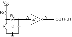
The input due to the push button switches multiple times, causing the output of a non Schmitt-trigger device to trigger multiple times, while the Schmitt-trigger input device with RC delay limits the output pulse to a single pulse desired by the user. The separated positive and negative input voltage threshold values, see Figure 9, prevent multiple triggers from occurring.
SN74LVC1G14 sces218_app1.gifFigure 8. Push Button Debounce Circuit Schematic