SCES560G March 2004 – June 2015 SN74LVC1G175
PRODUCTION DATA.
- 1 Features
- 2 Applications
- 3 Description
- 4 Revision History
- 5 Pin Configuration and Functions
-
6 Specifications
- 6.1 Absolute Maximum Ratings
- 6.2 ESD Ratings
- 6.3 Recommended Operating Conditions
- 6.4 Thermal Information
- 6.5 Electrical Characteristics
- 6.6 Timing Requirements, -40°C to 85°C
- 6.7 Timing Requirements, -40°C to 125°C
- 6.8 Switching Characteristics, -40°C to 85°C
- 6.9 Switching Characteristics, -40°C to 85°C
- 6.10 Switching Characteristics, -40°C to 125°C
- 6.11 Operating Characteristics
- 6.12 Typical Characteristics
- 7 Parameter Measurement Information
- 8 Detailed Description
- 9 Application and Implementation
- 10Power Supply Recommendations
- 11Layout
- 12Device and Documentation Support
- 13Mechanical, Packaging, and Orderable Information
封装选项
机械数据 (封装 | 引脚)
散热焊盘机械数据 (封装 | 引脚)
- DRY|6
订购信息
5 Pin Configuration and Functions
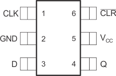
DBV Package
6-Pin SOT-23
Top View

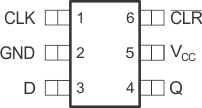
DCK Package
6-Pin SC70
Top View

DRY Package
6-Pin SON
Top View

YZP Package
6-Pin DSBGA
Bottom View

See mechanical drawings for dimensions.
Pin Functions
| PIN | I/O | DESCRIPTION | ||
|---|---|---|---|---|
| NAME | NO. | |||
| CLK | 1 | I | Clock Input | |
| CLR | 6 | I | Clear Data Input | |
| D | 3 | I | Data Input | |
| GND | 2 | — | Ground | |
| Q | 4 | O | Output | |
| VCC | 5 | — | Power | |