SCES528F December 2003 – May 2017 SN74LVC1G373
PRODUCTION DATA.
- 1 Features
- 2 Applications
- 3 Description
- 4 Revision History
- 5 Pin Configuration and Functions
-
6 Specifications
- 6.1 Absolute Maximum Ratings
- 6.2 ESD Ratings
- 6.3 Recommended Operating Conditions
- 6.4 Thermal Information
- 6.5 Electrical Characteristics
- 6.6 Timing Requirements: TA = -40°C to +85°C
- 6.7 Timing Requirements: TA = -40°C to +125°C
- 6.8 Switching Characteristics: TA = -40°C to +85°C
- 6.9 Switching Characteristics: TA = -40°C to +85°C
- 6.10 Switching Characteristics: TA = -40°C to +125°C
- 6.11 Operating Characteristics
- 6.12 Typical Characteristics
- 7 Parameter Measurement Information
- 8 Detailed Description
- 9 Application and Implementation
- 10Power Supply Recommendations
- 11Layout
- 12Device and Documentation Support
- 13Mechanical, Packaging, and Orderable Information
封装选项
请参考 PDF 数据表获取器件具体的封装图。
机械数据 (封装 | 引脚)
- DBV|6
- YZP|6
- DCK|6
散热焊盘机械数据 (封装 | 引脚)
订购信息
9 Application and Implementation
NOTE
Information in the following applications sections is not part of the TI component specification, and TI does not warrant its accuracy or completeness. TI’s customers are responsible for determining suitability of components for their purposes. Customers should validate and test their design implementation to confirm system functionality.
9.1 Application Information
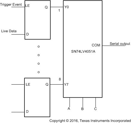
The SN74LVC1G373 latches can be used to store one bit of data. Figure 6 shows a typical application. The multiplexer is used to convert parallel data coming in from the latch into serial data using the A, B, and C select pins moving up in a sequence. With latch input low by a trigger event, the output Q holds the previous Q0 data entered until the LE pin is cleared.
9.2 Typical Application
 Figure 6. Latch Used With Multiplexer for Parallel to Serial Conversion
9.2.1 Design Requirements
This device uses CMOS technology and has balanced output drive. Take care to avoid bus contention because it can drive currents that would exceed maximum limits. The high drive also creates fast edges into light loads, so routing and load conditions must be considered to prevent ringing.
9.2.2 Detailed Design Procedure
- Recommended Input Conditions
- For rise time and fall time specifications, see Δt/ΔV in Recommended Operating Conditions.
- For specified High and low levels, see VIH and VIL in Recommended Operating Conditions.
- Inputs are overvoltage tolerant allowing them to go as high as 5.5 V at any valid VCC.
- Recommended Output Conditions
- Load currents should not exceed 32 mA per output and 100 mA total through the part.
- Outputs must not be pulled above VCC.
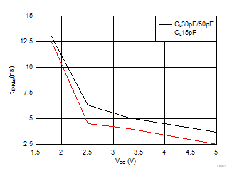
9.2.3 Application Curve
