SCES538G January 2004 – February 2020 SN74LVC1G38
PRODUCTION DATA.
- 1 Features
- 2 Applications
- 3 Description
- 4 Revision History
- 5 Pin Configuration and Functions
-
6 Specifications
- 6.1 Absolute Maximum Ratings
- 6.2 ESD Ratings
- 6.3 Recommended Operating Conditions
- 6.4 Thermal Information
- 6.5 Electrical Characteristics
- 6.6 Switching Characteristics, CL = 15 pF
- 6.7 Switching Characteristics, CL = 30 pF or 50 pF, –40°C to +85°C
- 6.8 Switching Characteristics, CL = 30 pF or 50 pF, –40°C to +125°C
- 6.9 Operating Characteristics
- 6.10 Typical Characteristics
- 7 Parameter Measurement Information
- 8 Detailed Description
- 9 Application and Implementation
- 10Power Supply Recommendations
- 11Layout
- 12Device and Documentation Support
- 13Mechanical, Packaging, and Orderable Information
封装选项
请参考 PDF 数据表获取器件具体的封装图。
机械数据 (封装 | 引脚)
- DPW|5
- DBV|5
- DSF|6
- DCK|5
- DRY|6
散热焊盘机械数据 (封装 | 引脚)
订购信息
5 Pin Configuration and Functions
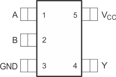
DBV Package
5-Pin SOT-23
Top View

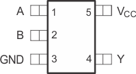
DCK Package
5-Pin SC70
Top View

DRY Package
6-Pin SON
Top View

NC – No internal connection.
DSF Package
6-Pin SON
Top View

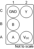
YZP Package
5-Pin DSBGA
Bottom View

See mechanical drawings for dimensions
DPW Package
5-Pin X2SON
Top View

Pin Functions
| PIN | I/O | DESCRIPTION | |||
|---|---|---|---|---|---|
| NAME | DBV, DCK, DPW | DRY, DSF | YZP | ||
| A | 1 | 1, 5 | A1 | I | Logic Input A |
| B | 2 | 2 | B1 | I | Logic Input B |
| GND | 3 | 3 | C1 | — | Ground |
| NC | — | 5 | — | — | No Internal Connection |
| Y | 4 | 4 | C2 | O | Output Y |
| VCC | 5 | 6 | A2 | — | Positive Supply |