SCES499E June 2001 – April 2015 SN74LVC1G66-Q1
PRODUCTION DATA.
- 1 Features
- 2 Applications
- 3 Description
- 4 Revision History
- 5 Pin Configuration and Functions
- 6 Specifications
- 7 Parameter Measurement Information
- 8 Detailed Description
- 9 Application and Implementation
- 10Power Supply Recommendations
- 11Layout
- 12Device and Documentation Support
- 13Mechanical, Packaging, and Orderable Information
8 Detailed Description
8.1 Overview
This single analog switch is designed for 1.65-V to 5.5-V VCC operation in automotive applications.
The SN74LVC1G66-Q1 device supports analog and digital signals. The device permits bidirectional transmission of signals with amplitudes of up to 5.5 V (peak). Like all analog switches, the SN74LVC1G66-Q1 is bidirectional.
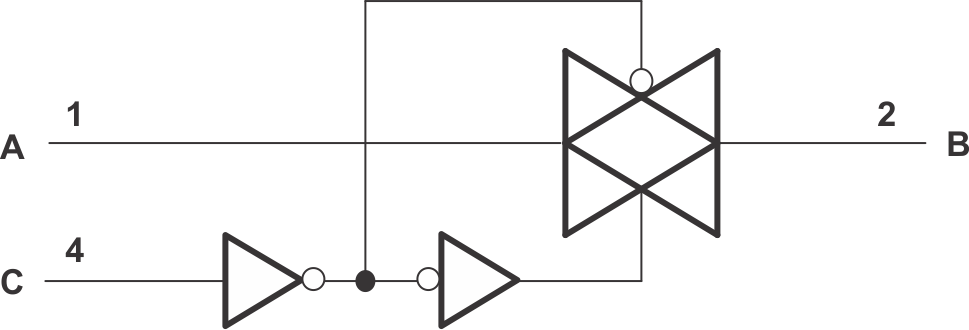
8.2 Functional Block Diagram
 Figure 10. Logic Diagram (Positive Logic)
8.3 Feature Description
This device is tested for operation in automotive applications. The SN74LVC1G66-Q1 has a wide VCC range, allowing rail-to-rail operation of signals anywhere from a 1.8-V system to a 5-V system. In addition, the control input (C Pin) is 5.5-V tolerant, allowing higher-voltage logic to interface to the switch control system.
8.4 Device Functional Modes
Table 1. Function Table
| CONTROL INPUT (C) | SWITCH |
|---|---|
| L | OFF |
| H | ON |