SCES323Q June 2001 – March 2017 SN74LVC1G66
PRODUCTION DATA.
- 1 Features
- 2 Applications
- 3 Description
- 4 Revision History
- 5 Pin Configuration and Functions
- 6 Specifications
- 7 Parameter Measurement Information
- 8 Detailed Description
- 9 Application and Implementation
- 10Power Supply Recommendations
- 11Layout
- 12Device and Documentation Support
- 13Mechanical, Packaging, and Orderable Information
封装选项
请参考 PDF 数据表获取器件具体的封装图。
机械数据 (封装 | 引脚)
- DBV|5
- DSF|6
- DCK|5
- DRL|5
- YZP|5
- DRY|6
散热焊盘机械数据 (封装 | 引脚)
- DRY|6
订购信息
8 Detailed Description
8.1 Overview
This single analog switch is designed for 1.65-V to 5.5-V VCC operation.
The SN74LVC1G66 device can handle analog and digital signals. The device permits bidirectional transmission of signals with amplitudes of up to 5.5 V (peak). Like all analog switches, the SN74LVC1G66 is bidirectional.
NanoFree package technology is a major breakthrough in IC packaging concepts, using the die as the package.
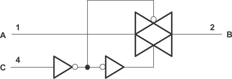
8.2 Functional Block Diagram
 Figure 10. Logic Diagram (Positive Logic)
8.3 Feature Description
The TI NanoFree package is one of TI’s smallest packages and allows customers to save board space while the solder bumps allow for easy testing. The SN74LVC1G66 has a wide VCC range, allowing rail-to-rail operation of signals anywhere from a 1.8-V system to a 5-V system. In addition, the control input (C Pin) is 5.5-V tolerant, allowing higher-voltage logic to interface to the switch control system.
8.4 Device Functional Modes
Table 1. Function Table
| CONTROL INPUT (C) | SWITCH |
|---|---|
| L | OFF |
| H | ON |