SCES323Q June 2001 – March 2017 SN74LVC1G66
PRODUCTION DATA.
- 1 Features
- 2 Applications
- 3 Description
- 4 Revision History
- 5 Pin Configuration and Functions
- 6 Specifications
- 7 Parameter Measurement Information
- 8 Detailed Description
- 9 Application and Implementation
- 10Power Supply Recommendations
- 11Layout
- 12Device and Documentation Support
- 13Mechanical, Packaging, and Orderable Information
封装选项
请参考 PDF 数据表获取器件具体的封装图。
机械数据 (封装 | 引脚)
- DBV|5
- DSF|6
- DCK|5
- DRL|5
- YZP|5
- DRY|6
散热焊盘机械数据 (封装 | 引脚)
- DRY|6
订购信息
5 Pin Configuration and Functions
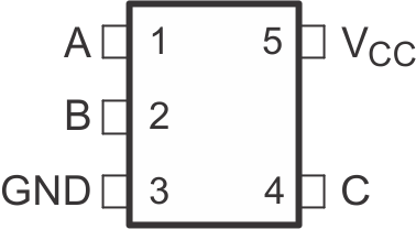
DCK Package
5-Pin SC70
(Top View)

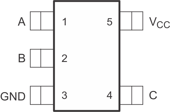
DRL Package
5-Pin SOT
(Top View)

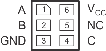
DSF Package
6-Pin X2SON
(Top View)

DRY Package
6-Pin USON
(Top View)

Pin Functions
| PIN | I/O | DESCRIPTION | ||
|---|---|---|---|---|
| NAME | SOT NO. | USON, X2SON NO. | ||
| A | 1 | 1 | I/O | Bidirectional signal to be switched |
| B | 2 | 2 | I/O | Bidirectional signal to be switched |
| C | 4 | 4 | I | Controls the switch (L = OFF, H = ON) |
| GND | 3 | 3 | — | Ground pin |
| NC | — | 5 | — | Do not connect |
| VCC | 5 | 6 | — | Power pin |
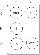
Pin Functions
| PIN | I/O | DESCRIPTION | |
|---|---|---|---|
| NAME | DSBGA NO. | ||
| A | A1 | I/O | Bidirectional signal to be switched |
| B | B1 | I/O | Bidirectional signal to be switched |
| C | C2 | I | Controls the switch (L = OFF, H = ON) |
| GND | C1 | — | Ground pin |
| VCC | A2 | — | Power pin |

