SCES581D JULY 2004 – October 2015 SN74LVC1GX04
UNLESS OTHERWISE NOTED, this document contains PRODUCTION DATA.
- 1 Features
- 2 Applications
- 3 Description
- 4 Revision History
- 5 Pin Configuration and Functions
-
6 Specifications
- 6.1 Absolute Maximum Ratings
- 6.2 ESD Ratings
- 6.3 Recommended Operating Conditions
- 6.4 Thermal Information
- 6.5 Electrical Characteristics
- 6.6 Switching Characteristics, SN74LVC1GX04
- 6.7 Switching Characteristics, SN74LVC1GX04
- 6.8 Switching Characteristics, SN74LVC1GX04
- 6.9 Operating Characteristics
- 6.10 Typical Characteristics
- 7 Parameter Measurement Information
- 8 Detailed Description
- 9 Application and Implementation
- 10Power Supply Recommendations
- 11Layout
- 12Device and Documentation Support
- 13Mechanical, Packaging, and Orderable Information
封装选项
请参考 PDF 数据表获取器件具体的封装图。
机械数据 (封装 | 引脚)
- DBV|6
- DRL|6
- DCK|6
散热焊盘机械数据 (封装 | 引脚)
订购信息
9 Application and Implementation
NOTE
Information in the following applications sections is not part of the TI component specification, and TI does not warrant its accuracy or completeness. TI’s customers are responsible for determining suitability of components for their purposes. Customers should validate and test their design implementation to confirm system functionality.
9.1 Application Information
The SN74LVC1GX04 contains a buffered and unbuffered inverter for the specific purpose of creating a crystal oscillator and driver with limited external components.
9.2 Typical Application
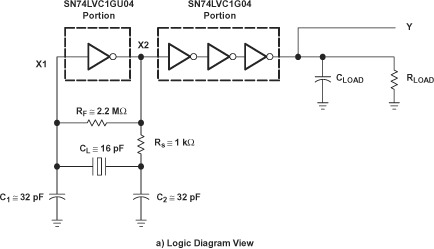
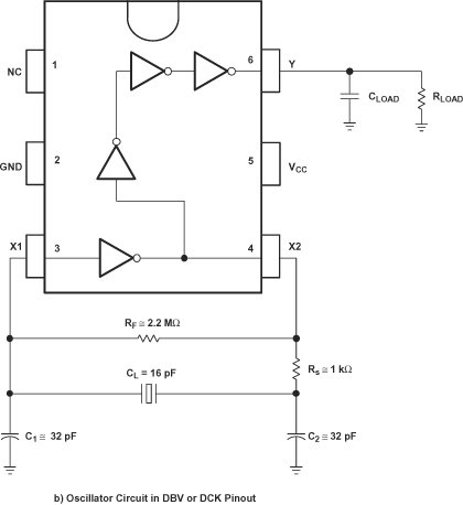
Figure 5 shows a typical application of the SN74LVC1GX04 in a Pierce oscillator circuit. The buffered inverter (SN74LVC1G04 portion) produces a rail-to-rail voltage waveform. The recommended load for the crystal shown in this example is 16 pF. The value of the recommended load (CL) can be found in the crystal manufacturer's data sheet.
Values of C1 and C2 are chosen to calculate CL in Equation 1 where C1 ≡ C2.

Rs is the current-limiting resistor, and the value depends on the maximum power dissipation of the crystal. Generally, the recommended value of Rs is specified in the crystal manufacturer's data sheet and, usually, this value is approximately equal to the reactance of C2 at resonance frequency, that is seen in Equation 2.

RF is the feedback resistor that is used to bias the inverter in the linear region of operation. Usually, the value is chosen to be within 1 MΩ to 10 MΩ.
 Figure 5. Oscillator Circuit
 Figure 6. Oscillator Circuit (Continued)
9.2.1 Design Requirements
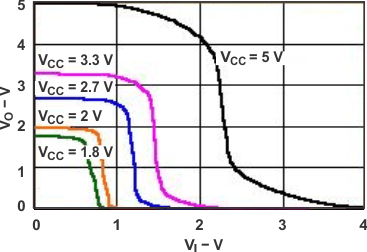
The open-loop gain of the unbuffered inverter decreases as power-supply voltage decreases. This decreases the closed-loop gain of the oscillator circuit. The value of Rs can be decreased to increase the closed-loop gain, while maintaining the power dissipation of the crystal within the maximum limit.
Rs and C2 form a low-pass filter and reduce spurious oscillations. Component values can be adjusted, based on the desired cutoff frequency.
C2 can be increased over C1 to increase the phase shift and help in start-up of the oscillator. Increasing C2 may affect the duty cycle of the output voltage.
At high frequency, phase shift due to Rs becomes significant. In this case, Rs can be replaced by a capacitor to reduce the phase shift.
9.2.2 Detailed Design Procedure
After the selection of proper component values, the oscillator circuit should be tested using these components. To ensure that the oscillator circuit performs within the Recommended Operating Conditions, follow these steps:
- Without a crystal, the oscillator circuit should not oscillate. To check this, the crystal can be replaced by its equivalent parallel-resonant resistance.
- When the power-supply voltage drops, the closed-loop gain of the oscillator circuit reduces. Ensure that the circuit oscillates at the appropriate frequency at the lowest VCC and highest VCC.
- Ensure that the duty cycle, start-up time, and frequency drift over time is within the system requirements.
9.2.3 Application Curve
 Figure 7. VO vs VI Characteristics of Oscillator Amplifier