ZHCSI94N July 2001 – August 2018 SN74LVC2G66
PRODUCTION DATA.
- 1 特性
- 2 应用
- 3 说明
- 4 修订历史记录
- 5 Pin Configuration and Functions
- 6 Specifications
- 7 Parameter Measurement Information
- 8 Detailed Description
- 9 Application and Implementation
- 10Power Supply Recommendations
- 11Layout
- 12器件和文档支持
- 13机械、封装和可订购信息
封装选项
请参考 PDF 数据表获取器件具体的封装图。
机械数据 (封装 | 引脚)
- DCU|8
- YZP|8
- DCT|8
散热焊盘机械数据 (封装 | 引脚)
订购信息
7 Parameter Measurement Information
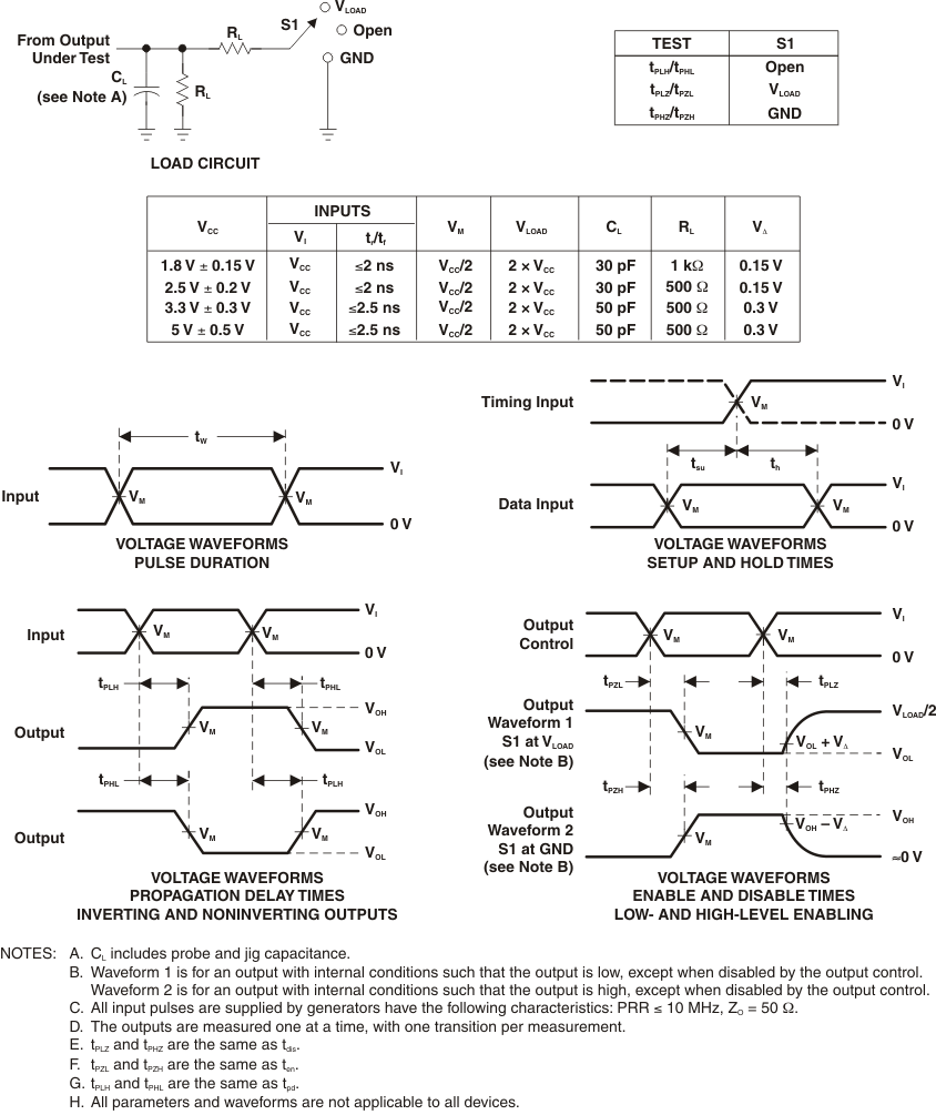 Figure 2. Load Circuit and Voltage Waveforms
 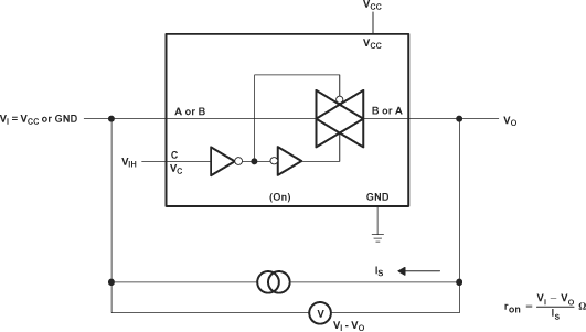 Figure 3. ON-State Resistance Test Circuit
 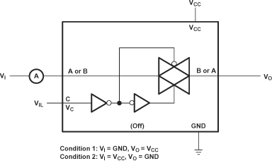 Figure 4. OFF-State Switch Leakage-Current Test Circuit
 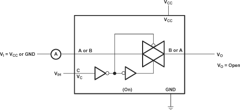 Figure 5. ON-State Leakage-Current Test Circuit
 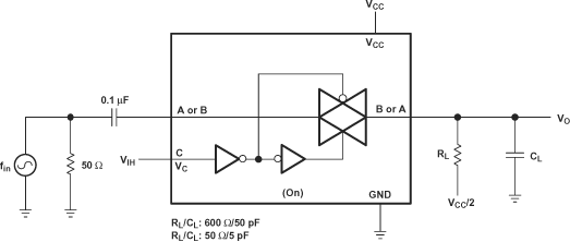 Figure 6. Frequency Response (Switch On)
 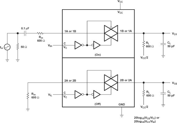 Figure 7. Crosstalk (Between Switches)
 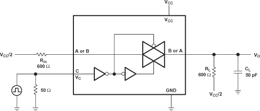 Figure 8. Crosstalk (Control Input, Switch Output)
 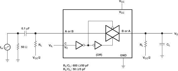 Figure 9. Feedthrough (Switch Off)
 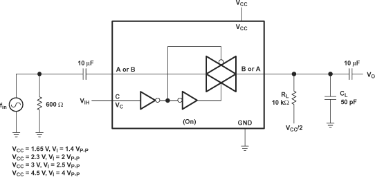 Figure 10. Sine-Wave Distortion