SCES366L August 2001 – October 2015 SN74LVC3G34
PRODUCTION DATA.
- 1 Features
- 2 Applications
- 3 Description
- 4 Revision History
- 5 Pin Configuration and Functions
- 6 Specifications
- 7 Parameter Measurement Information
- 8 Detailed Description
- 9 Application and Implementation
- 10Power Supply Recommendations
- 11Layout
- 12Device and Documentation Support
- 13Mechanical, Packaging, and Orderable Information
封装选项
请参考 PDF 数据表获取器件具体的封装图。
机械数据 (封装 | 引脚)
- DCU|8
- YZP|8
- DCT|8
散热焊盘机械数据 (封装 | 引脚)
订购信息
8 Detailed Description
8.1 Overview
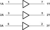
The SN74LVC3G34 device contains three buffer gates that each perform the Boolean function Y = A. This device is fully specified for partial-power-down applications using Ioff. The Ioff circuitry disables the outputs, preventing damaging current backflow through the device when it is powered down.
8.2 Functional Block Diagram

8.3 Feature Description
The SN74LVC3G34 device has a wider operating voltage range, operating from 1.65 V to 5.5 V, and allows down voltage translation. The SN74LVC3G34 Ioff feature allows voltages on the inputs and outputs when VCC is
0 V.
8.4 Device Functional Modes
Table 1 lists the functional modes of the SN74LVC3G34.
Table 1. Function Table
| INPUT A |
OUTPUT Y |
|---|---|
| H | H |
| L | L |