ZHCSLJ9E October   1998  – July 2020 SN74LVCH32373A

PRODUCTION DATA  

  1. 特性
  2. 应用
  3. 说明
  4. Revision History
  5. Pin Configuration and Functions
    1.     6
  6. Specifications
    1. 6.1 Absolute Maximum Ratings
    2. 6.2 ESD Ratings
    3. 6.3 Recommended Operating Conditions
    4. 6.4 Thermal Information
    5. 6.5 Electrical Characteristics
    6. 6.6 Timing Requirements
    7. 6.7 Switching Characteristics
    8. 6.8 Operating Characteristics
    9. 6.9 Typical Characteristics
  7. Detailed Description
    1. 7.1 Overview
    2. 7.2 Functional Block Diagram
    3. 7.3 Feature Description
      1. 7.3.1 Standard CMOS Inputs
      2. 7.3.2 Balanced High-Drive CMOS Push-Pull Outputs
      3. 7.3.3 Partial Power Down (Ioff)
      4. 7.3.4 Over-voltage Tolerant Inputs
      5. 7.3.5 Clamp Diode Structure
      6. 7.3.6 Bus-Hold Data Inputs
    4. 7.4 Device Functional Modes
  8. Application and Implementation
    1. 8.1 Application Information
    2. 8.2 Typical Application
      1. 8.2.1 Design Requirements
        1. 8.2.1.1 Power Considerations
        2. 8.2.1.2 Input Considerations
        3. 8.2.1.3 Output Considerations
        4. 8.2.1.4 Timing Considerations
      2. 8.2.2 Detailed Design Procedure
      3. 8.2.3 Application Curves
  9. Power Supply Recommendations
  10. 10Layout
    1. 10.1 Layout Guidelines
    2. 10.2 Layout Example
  11. 11Device and Documentation Support
    1. 11.1 Documentation Support
      1. 11.1.1 Related Documentation
    2. 11.2 Support Resources
    3. 11.3 Trademarks
    4. 11.4 Electrostatic Discharge Caution
    5. 11.5 Glossary
  12. 12Mechanical, Packaging, and Orderable Information

封装选项

请参考 PDF 数据表获取器件具体的封装图。

机械数据 (封装 | 引脚)
  • NMJ|96
散热焊盘机械数据 (封装 | 引脚)
订购信息

Bus-Hold Data Inputs

Each data input (D) on this device includes a weak latch that maintains a valid logic level on the input. The state of these latches is unknown at startup and remains unknown until the input has been forced to a valid high or low state. After data has been sent through a channel, the latch then maintains the previous state on the input if the line is left floating. It is not recommended to use pull-up or pull-down resistors together with a bus-hold input, as it may cause undefined inputs to occur which can lead to excessive current consumption.

Bus-hold data inputs prevent floating inputs on this device. The Implications of Slow or Floating CMOS Inputs application report explains the problems associated with leaving CMOS inputs floating. These latches remain active at all times, independent of all control signals such as direction control or output enable. The Bus-Hold Circuit application report has additional details regarding bus-hold inputs.
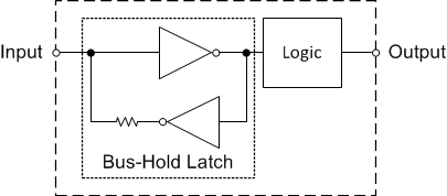
GUID-896320F2-F124-439C-A22D-A4A9BD2162E9-low.gifFigure 7-2 Bus-Hold circuit block diagram representation