ZHCSNT1J February 1997 – August 2022 SN65220 , SN65240 , SN75240
PRODUCTION DATA
- 1 特性
- 2 应用
- 3 说明
- 4 Revision History
- 5 Device Comparison Table
- 6 Pin Configuration and Functions
- 7 Specifications
- 8 Parameter Measurement Information
- 9 Detailed Description
- 10Application and Implementation
- 11Power Supply Recommendations
- 12Layout
- 13Device and Documentation Support
- 14Mechanical, Packaging, and Orderable Information
9.1 Overview
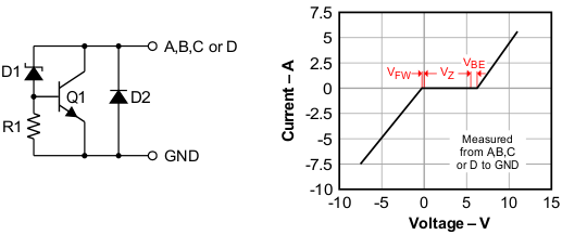
The SN65220, SN65240, and SN75240 devices integrate multiple unidirectional transient voltage suppressors (TVS). Figure 9-1 shows the equivalent circuit diagram of a single TVS diode.
For positive transient voltages, only the Q1 transistor determines the switching characteristic. When the input voltage reaches the Zener voltage, VZ, Zener diode D1 conducts; therefore, allowing for the base-emitter voltage, VBE, to increase. At VIN = VZ + VBE, the transistor starts conducting. From then on, its on-resistance decreases linearly with increasing input voltage.
For negative transient voltages, only diode D2 determines the switching characteristic. Here, switching occurs when the input voltage exceeds the diode forward voltage, VFW.
 Figure 9-1 TVS Structure and Current — Voltage Characteristic