SLLS362G SEPTEMBER 1999 – January 2016 SN65LVDS387 , SN65LVDS389 , SN65LVDS391 , SN75LVDS387 , SN75LVDS389 , SN75LVDS391
PRODUCTION DATA.
- 1 Features
- 2 Applications
- 3 Description
- 4 Revision History
- 5 Description (Continued)
- 6 Device Options
- 7 Pin Configuration and Functions
- 8 Specifications
- 9 Parameter Measurement Information
- 10Detailed Description
- 11Application and Implementation
- 12Power Supply Recommendations
- 13Layout
- 14Device and Documentation Support
- 15Mechanical, Packaging, and Orderable Information
10 Detailed Description
10.1 Overview
The SNx5LVDSxx devices are quad-, eight-, and 16-channel LVDS line drivers. They operate from a single supply that is nominally 3.3 V, but can be as low as 3 V and as high as 3.6 V. The input signals to the SNx5LVDSxx device are LVTTL signals. The outputs of the device are differential signals complying with the LVDS standard (TIA/EIA-644A). The differential output signal operates with a signal level of 340 mV, nominally, at a common-mode voltage of 1.2 V. This low differential output voltage results in a low emitted radiated energy, which is dependent on the signal slew rate. The differential nature of the output provides immunity to common-mode coupled signals.
The SNx5LVDSxx device is intended to drive a 100-Ω transmission line. This transmission line may be a printed-circuit board (PCB) or cabled interconnect. With transmission lines, the optimum signal quality and power delivery is reached when the transmission line is terminated with a load equal to the characteristic impedance of the interconnect. Likewise, the driven 100-Ω transmission line should be terminated with a matched resistance.
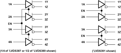
10.2 Functional Block Diagram
 Figure 14. Logic Diagram (Positive Logic)
10.3 Feature Description
10.3.1 Driver Output Voltage and Power-On Reset
The SNx5LVDSxx driver operates and meets all the specified performance requirements for supply voltages in the range of 3.0 V to 3.6 V. When the supply voltage drops below 1.5 V (or is turning on and has not yet reached 1.5 V), power-on reset circuitry sets the driver output to a high-impedance state.
10.3.2 5-V Input Tolerance
5-V and 3.3-V TTL logic standards share the same input high-voltage and input low-voltage thresholds, namely 2.0 V and 0.8 V, respectively. Although the maximum supply voltage for the SNx5LVDSxx is 3.6 V, the driver can operate and meet all performance requirements when the input signals are as high as 5 V. This allows operation with 3.3-V TTL as well as 5-V TTL logic. 3.3-V CMOS and 5-V CMOS inputs are also allowable, although one should ensure that the duty-cycle distortion that will result from the TTL (ground-referenced) thresholds are acceptable.
10.3.3 NC Pins
NC (not connected) pins are pins where the die is not physically connected to the lead frame or package. For optimum thermal performance, a good rule of thumb is to ground the NC pins at the board level.
10.3.4 Unused Enable Pins
Unused enable pins should be tied to VCC or GND as appropriate.
10.3.5 Driver Equivalent Schematics
The SNx5LVDSxx equivalent output schematic diagrams are shown in Figure 15. The driver input is represented by a CMOS inverter stage with a 7-V Zener diode. The input stage is high-impedance, and includes an internal pulldown to ground. If the driver input is left open, the driver input provides a low-level signal to the rest of the driver circuitry, resulting in a low-level signal at the driver output pins. The Zener diode provides ESD protection. The driver output stage is a differential pair, one half of which is shown in Figure 15. Like the input stage, the driver output includes Zener diodes for ESD protection. The schematic shows an output stage that includes a set of current sources (nominally 3.5 mA) that are connected to the output load circuit based upon the input stage signal. To the first order, the SNx5LVDSxx output stage acts a constant-current source.
 Figure 15. Equivalent Input and Output Schematic Diagrams