SNLS666 January 2020 SN75LVPE4410
PRODUCTION DATA.
- 1 Features
- 2 Applications
- 3 Description
- 4 Revision History
- 5 Pin Configuration and Functions
- 6 Specifications
- 7 Detailed Description
- 8 Application and Implementation
- 9 Power Supply Recommendations
- 10Layout
- 11Device and Documentation Support
- 12Mechanical, Packaging, and Orderable Information
8.2.1.3 Application Curves
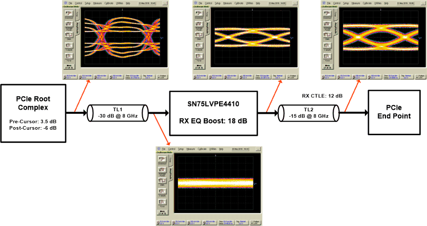
The SN75LVPE4410 is a linear redriver that can be used to extend channel reach of a PCIe link. Normally, PCIe-compliant TX and RX are equipped with signal-conditioning functions and can handle channel losses of up to 28 dB at 8 GHz. With the SN75LVPE4410, the total channel loss between a PCIe root complex and an end point can be up to 45 dB at 8 GHz.
Figure 11 shows an electric link that models a single channel of a PCIe link and eye diagrams measured at different locations along the link. The source that models a PCIe TX sends a 16 Gbps PRBS-15 signal with P7 presets. After a transmission channel with –30 dB at 8-GHz insertion loss, the eye diagram is fully closed. The SN75LVPE4410 with its CTLE set to the maximum (18 dB boost) together with the source TX equalization compensates for the losses of the pre-channel (TL1) and opens the eye at the output of the SN75LVPE4410.
The post-channel (TL2) losses mandate the use of PCIe RX equalization functions such as CTLE and DFE that are normally available in PCIe compliant receivers.
 Figure 11. PCIe Gen 4.0 Link Reach Extension Using SN75LVPE4410