SLASFC6 August 2024 TAS2120
ADVANCE INFORMATION
- 1
- 1 Features
- 2 Applications
- 3 Description
- 4 Pin Configuration and Functions
- 5 Specifications
-
6 Detailed Description
- 6.1 Overview
- 6.2 Functional Block Diagram
- 6.3 Device Functional Modes
- 6.4 Feature Description
- 6.5 Programming
- 7 Application and Implementation
- 8 Power Supply Recommendations
- 9 Layout
- 10Device and Documentation Support
- 11Revision History
- 12Mechanical, Packaging, and Orderable Information
6.4.4 Boost
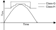
The TAS2120 internal processing algorithm automatically enables the boost when needed. A look-ahead algorithm monitors the battery voltage and the digital audio stream. When the speaker output approaches the battery voltage the boost is enabled in-time to supply the required speaker output voltage. When the boost is no longer required it is disabled and bypassed to maximize efficiency. The boost can be configured in one of two modes. The first is low in-rush (Class-G) supporting only boost on-off and has the lowest in-rush current. The second is high-efficiency (Class-H) where the boost voltage level is adjusted to a value just above what is needed. This mode is more efficient but has a higher in-rush current to quickly transition the levels. This can be configured using BST_MODE[1:0] register bits.
 Figure 6-9 Boost Mode Signal
Tracking Example
Figure 6-9 Boost Mode Signal
Tracking Example| BST_MODE[1:0] | BOOST MODE |
|---|---|
| 00 | Class-H - High efficiency (default) |
| 01 | Class-G - Low in-rush |
| 10 | Always On |
| 11 | Always Off - Pass-through |
The boost can be enabled and disabled using BST_EN register. When driving the Class-D amplifier using an external supply through the PVDD pin, the boost should be disabled and the SW pin should be left floating.
| BST_EN | BOOST IS |
|---|---|
| 0 | Disabled (External PVDD mode) |
| 1 | Enabled (default) |
The maximum boost voltage is set by VBOOST_MAX_CTRL[7:0]. When operating in class-G mode, the boost when needed will be at this voltage. In class-H mode of operation the boost voltage is automatically selected based on the audio signal but will not exceed this set value. In class-H mode, the class-H controller controls the Boost with a minimum step size of 33mV to generate the required PVDD voltage. The max boost voltage that the device generates is controlled by VBOOST_MAX_CTRL[7:0] and it can be configured with a step size of 66mV.
| VBOOST_MAX_CTRL[7:0] | BOOST VOLTAGE (V) |
|---|---|
| 0x00 - 0x53 | Reserved |
| 0x54 | 5.54 V |
| 0x55 | 5.61 V |
| ... | …..steps of 66mV per LSB step …... |
| 0xA7 | 11.02 V (default) |
| ... | …..steps of 66mV per LSB step …... |
| 0xE0 | 14.75V |
| 0xE6 - 0xFF | Reserved |
| BST_MIN_FREQ_SEL[1:0] | LOWER LIMIT |
|---|---|
| 00 | No lower limit (default) |
| 01 | 25 kHz |
| 10 | 50 kHz |
| 11 | RESERVED |
The peak current drawn by the boost is controlled using BST_ILIM[23:0] register and it limits the current drawn from the VBAT supply. This setting allows flexibility in the inductor selection for various saturation currents. The system should always use inductors which have minimum saturation current (ISAT) atleast 5% higher than programmed BST_ILIM setting. The Boost circuit can go unstable if the inductor's ISAT is lower than the BST_ILIM setting. The current limit can be adjusted in 39.1 mA steps with a range from 1.5A to 5.1A using PPC3 Software.
The change in boost configurations like BST_ILIM, VBOOST_MAX_CTRL etc requires re-tuning of device parameters such as CLASSH_TUNING_xx[23:0] registers to achieve best performance while ensuring no functionality failures. This configuration should be changed using PPC3 tool to enable automatic reconfiguration of all the associated device parameters.
For multiple channel systems, the boost phase can be shifted to ensure each device will draw peak current from the battery at different instance of times and enable lower instantaneous peak current from the battery. The boost syncing among multiple devices is enabled using BOOST_PHASE_SYNC_EN. The individual device boost phase can be automatically configured to different values using the i2c target address device detected by using BOOST_PHASE_FROM_ADDRESS_PIN register, or it can be manually configured using BOOST_PHASE register. The Boost phase shift is done by each device using the FSYNC pulse to synchronize each device and all the devices which require the Boost phase synchronization should be connected to same FSYNC from the host in the system.
| BOOST_PHASE_SYNC_EN | Status |
|---|---|
| 0 | Disabled |
| 1 | Enabled(default) |
| BOOST_PHASE_FROM_ADDRESS_PIN | Status |
|---|---|
| 0 | Disabled |
| 1 | Enabled(default) |
| BOOST_PHASE[1:0] | Phase Delay |
|---|---|
| 00 | Phase shift is 0ns (default) |
| 01 | Phase shift is 65ns (~90° for max clock) |
| 10 | Phase shift is 130ns (~180° for max clock) |
| 11 | Phase shift is 195ns (~270° for max clock) |