ZHCSGI2E july   2017  – july 2023 TAS2505-Q1

PRODUCTION DATA  

  1.   1
  2. 特性
  3. 应用
  4. 说明
  5. Revision History
  6. Pin Configuration and Functions
  7. Specifications
    1. 6.1  Absolute Maximum Ratings
    2. 6.2  ESD Ratings
    3. 6.3  Recommended Operating Conditions
    4. 6.4  Thermal Information
    5. 6.5  Electrical Characteristics
    6. 6.6  I2S/LJF/RJF Timing in Master Mode
    7. 6.7  I2S/LJF/RJF Timing in Slave Mode
    8. 6.8  DSP Timing in Master Mode
    9. 6.9  DSP Timing in Slave Mode
    10. 6.10 I2C Interface Timing
    11. 6.11 SPI Interface Timing
    12. 6.12 Typical Characteristics
      1. 6.12.1 Class D Speaker Driver Performance
      2. 6.12.2 HP Driver Performance
  8. Parameter Measurement Information
  9. Detailed Description
    1. 8.1 Overview
    2. 8.2 Functional Block Diagram
    3. 8.3 Feature Description
      1. 8.3.1 Audio Analog I/O
      2. 8.3.2 Audio DAC and Audio Analog Outputs
      3. 8.3.3 DAC
      4. 8.3.4 POR
      5. 8.3.5 CLOCK Generation and PLL
      6. 8.3.6 Speaker Driver
      7. 8.3.7 Automotive Diagnostics
    4. 8.4 Device Functional Modes
      1. 8.4.1 Digital Pins
      2. 8.4.2 Analog Pins
      3. 8.4.3 Multifunction Pins
      4. 8.4.4 Analog Signals
        1. 8.4.4.1 Analog Inputs AINL and AINR
      5. 8.4.5 DAC Processing Blocks — Overview
      6. 8.4.6 Digital Mixing and Routing
      7. 8.4.7 Analog Audio Routing
      8. 8.4.8 5V LDO
      9. 8.4.9 Digital Audio and Control Interface
        1. 8.4.9.1 Digital Audio Interface
        2. 8.4.9.2 Control Interface
          1. 8.4.9.2.1 I2C Control Mode
          2. 8.4.9.2.2 SPI Digital Interface
        3. 8.4.9.3 Device Special Functions
    5. 8.5 Register Map
  10. Application and Implementation
    1. 9.1 Application Information
    2. 9.2 Typical Applications
      1. 9.2.1 Typical Configuration
        1. 9.2.1.1 Design Requirements
        2. 9.2.1.2 Detailed Design Procedure
        3. 9.2.1.3 Application Curves
      2. 9.2.2 Circuit Configuration With Internal LDO
        1. 9.2.2.1 Design Requirements
  11. 10Power Supply Recommendations
  12. 11Layout
    1. 11.1 Layout Guidelines
    2. 11.2 Layout Example
    3. 11.3 Thermal Pad
  13. 12Device and Documentation Support
    1. 12.1 Documentation Support
      1. 12.1.1 Related Documentation
    2. 12.2 Receiving Notification of Documentation Updates
    3. 12.3 Community Resources
    4. 12.4 Trademarks
  14. 13Mechanical, Packaging, and Orderable Information

封装选项

机械数据 (封装 | 引脚)
散热焊盘机械数据 (封装 | 引脚)
订购信息

Thermal Pad

Solder the Thermal PAD to GND plane. The plane will work as heat sink. For details about the corner pads size and location, refer to the Section 13 at the end of this document.
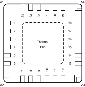
GUID-531BDF8E-68FE-4CE5-9265-95DFC8DF9796-low.gifFigure 11-2 Thermal Pad Corner Locations
Table 11-1 Thermal Pad Corner
CORNERDESCRIPTION
A1Internally connected to thermal pad. Leave floating or connect to the same plane as thermal pad.
A2
A3
A4